- 您現(xiàn)在的位置:買賣IC網(wǎng) > PDF目錄384536 > ISPGDX80VA-3T100 (LATTICE SEMICONDUCTOR CORP) In-System Programmable 3.3V Generic Digital CrosspointTM PDF資料下載
參數(shù)資料
| 型號: | ISPGDX80VA-3T100 |
| 廠商: | LATTICE SEMICONDUCTOR CORP |
| 元件分類: | PLD |
| 英文描述: | In-System Programmable 3.3V Generic Digital CrosspointTM |
| 中文描述: | EE PLD, 3 ns, PQFP100 |
| 封裝: | TQFP-100 |
| 文件頁數(shù): | 11/27頁 |
| 文件大?。?/td> | 346K |
| 代理商: | ISPGDX80VA-3T100 |
第1頁第2頁第3頁第4頁第5頁第6頁第7頁第8頁第9頁第10頁當前第11頁第12頁第13頁第14頁第15頁第16頁第17頁第18頁第19頁第20頁第21頁第22頁第23頁第24頁第25頁第26頁第27頁
11
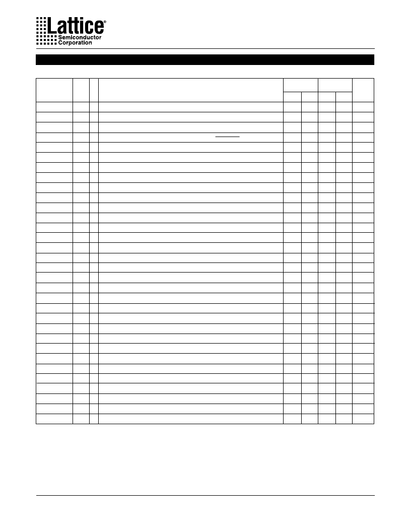
Specifications
ispGDX80VA
5.0
5.0
–
–
–
–
–
–
–
–
–
–
–
–
–
–
–
–
5.0
8.5
6.0
9.5
6.0
6.0
6.0
6.0
–
–
14.0
–
5.0
0.5
1
2
3
4
5
6
7
8
9
10
11
12
13
14
15
16
17
18
19
20
21
22
23
24
25
26
27
28
29
30
31
32
Data Prop. Delay from Any I/O pin to Any I/O Pin (4:1 MUX)
Data Prop. Delay from MUXsel Inputs to Any Output (4:1 MUX)
Clock Frequency, Max. Toggle
Clock Frequency with External Feedback
Input Latch or Register Setup Time Before Y
x
Input Latch or Register Setup Time Before I/O Clock
Output Latch or Register Setup Time Before Y
x
Output Latch or Register Setup Time Before I/O Clock
Global Clock Enable Setup Time Before Y
x
Global Clock Enable Setup Time Before I/O Clock
I/O Clock Enable Setup Time Before Y
x
Input Latch or Reg. Hold Time (Y
x
)
Input Latch or Reg. Hold Time (I/O Clock)
Output Latch or Reg. Hold Time (Y
x
)
Output Latch or Reg. Hold Time (I/O Clock)
Global Clock Enable Hold Time (Y
x
)
Global Clock Enable Hold Time (I/O Clock)
I/O Clock Enable Hold Time (Y
x
)
Output Latch or Reg. Clock (from Y
x
) to Output Delay
Input Latch or Register Clock (from Y
x
) to Output Delay
Output Latch or Register Clock (from I/O pin) to Output Delay
Input Latch or Register Clock (from I/O pin) to Output Delay
Input to Output Enable
Input to Output Disable
Test OE Output Enable
Test OE Output Disable
Clock Pulse Duration, High
Clock Pulse Duration, Low
Register Reset Delay from RESET Low
Reset Pulse Width
Output Delay Adder for Output Timings Using Slow Slew Rate
Output Skew (tgco1 Across Chip)
1. All timings measured with one output switching, fast output slew rate setting, except
t
sl
.
2. The delay parameters are measured with Vcc as I/O voltage reference. An additional 0.5ns delay is incurred when Vccio is
used as I/O voltage reference.
External Timing Parameters
Over Recommended Operating Conditions
ns
ns
MHz
MHz
ns
ns
ns
ns
ns
ns
ns
ns
ns
ns
ns
ns
ns
ns
ns
ns
ns
ns
ns
ns
ns
ns
ns
ns
ns
ns
ns
ns
–
–
143
111
4.0
3.0
4.0
3.0
2.5
1.5
4.5
0.0
1.5
0.0
1.5
0.0
1.5
0.0
–
–
–
–
–
–
–
–
3.5
3.5
–
10.0
–
–
A
A
–
–
–
–
–
–
–
–
–
–
–
–
–
–
–
–
A
A
A
A
B
C
B
C
–
–
–
–
D
A
t
pd
2
t
sel
2
f
max (Tog.)
f
max (Ext.)
t
su1
t
su2
t
su3
t
su4
t
suce1
t
suce2
t
suce3
t
h1
t
h2
t
h3
t
h4
t
hce1
t
hce2
t
hce3
t
gco1
2
t
gco2
2
t
co1
2
t
co2
2
t
en
2
t
dis
2
t
toeen
2
t
toedis
2
t
wh
t
wl
t
rst
t
rw
t
sl
t
sk
DESCRIPTION
PARAMETER
( )
1
UNITS
-5
MIN. MAX.
#
3.5
3.5
–
–
–
–
–
–
–
–
–
–
–
–
–
–
–
–
3.5
6.0
4.0
7.0
5.0
5.0
6.0
6.0
–
–
8.0
–
3.5
0.5
–
–
250
166.7
3.0
2.5
2.5
2.0
2.5
1.5
3.0
0.0
0.5
0.0
1.0
0.0
1.0
0.0
–
–
–
–
–
–
–
–
2.0
2.0
–
5.0
–
–
-3
MIN. MAX.
TEST
1
COND.
相關PDF資料 |
PDF描述 |
|---|---|
| ISPGDX80VA-5T100 | In-System Programmable 3.3V Generic Digital CrosspointTM |
| ISPGDX80VA-5T100I | In-System Programmable 3.3V Generic Digital CrosspointTM |
| ISPGDX80VA-7T100I | PHOTOELECTRIC PRODUCTS |
| ISPGDX80VA-9T100I | In-System Programmable 3.3V Generic Digital CrosspointTM |
| ISPL1048E-125LQI | High-Density Programmable Logic |
相關代理商/技術(shù)參數(shù) |
參數(shù)描述 |
|---|---|
| ISPGDX80VA3T100-5I | 制造商:Lattice Semiconductor Corporation 功能描述: |
| ISPGDX80VA-3TN100 | 功能描述:模擬和數(shù)字交叉點 IC PROGRAMMABLE GEN DIG CROSSPOINT RoHS:否 制造商:Micrel 配置:2 x 2 封裝 / 箱體:MLF-16 數(shù)據(jù)速率:10.7 Gbps 輸入電平:CML, LVDS, LVPECL 輸出電平:CML 電源電壓-最大:3.6 V 電源電壓-最小:2.375 V 最大工作溫度:+ 85 C 最小工作溫度:- 40 C 產(chǎn)品:Digital Crosspoint 封裝:Tube |
| ISPGDX80VA5T100 | 制造商:Lattice Semiconductor Corporation 功能描述: |
| ISPGDX80VA-5T100 | 功能描述:模擬和數(shù)字交叉點 IC PROGRAMMABLE GEN DIG CROSSPOINT RoHS:否 制造商:Micrel 配置:2 x 2 封裝 / 箱體:MLF-16 數(shù)據(jù)速率:10.7 Gbps 輸入電平:CML, LVDS, LVPECL 輸出電平:CML 電源電壓-最大:3.6 V 電源電壓-最小:2.375 V 最大工作溫度:+ 85 C 最小工作溫度:- 40 C 產(chǎn)品:Digital Crosspoint 封裝:Tube |
| ISPGDX80VA-5T100I | 功能描述:模擬和數(shù)字交叉點 IC PROGRAMMABLE GEN DIG CROSSPOINT RoHS:否 制造商:Micrel 配置:2 x 2 封裝 / 箱體:MLF-16 數(shù)據(jù)速率:10.7 Gbps 輸入電平:CML, LVDS, LVPECL 輸出電平:CML 電源電壓-最大:3.6 V 電源電壓-最小:2.375 V 最大工作溫度:+ 85 C 最小工作溫度:- 40 C 產(chǎn)品:Digital Crosspoint 封裝:Tube |
發(fā)布緊急采購,3分鐘左右您將得到回復。