- 您現(xiàn)在的位置:買賣IC網(wǎng) > PDF目錄370740 > HY5R288HC -|2.5V|8K|40|Direct RDRAM - 288M PDF資料下載
參數(shù)資料
| 型號(hào): | HY5R288HC |
| 英文描述: | -|2.5V|8K|40|Direct RDRAM - 288M |
| 中文描述: | - |為2.5V | 8K的| 40 |直接RDRAM的- 288M |
| 文件頁數(shù): | 47/64頁 |
| 文件大?。?/td> | 4542K |
| 代理商: | HY5R288HC |
第1頁第2頁第3頁第4頁第5頁第6頁第7頁第8頁第9頁第10頁第11頁第12頁第13頁第14頁第15頁第16頁第17頁第18頁第19頁第20頁第21頁第22頁第23頁第24頁第25頁第26頁第27頁第28頁第29頁第30頁第31頁第32頁第33頁第34頁第35頁第36頁第37頁第38頁第39頁第40頁第41頁第42頁第43頁第44頁第45頁第46頁當(dāng)前第47頁第48頁第49頁第50頁第51頁第52頁第53頁第54頁第55頁第56頁第57頁第58頁第59頁第60頁第61頁第62頁第63頁第64頁
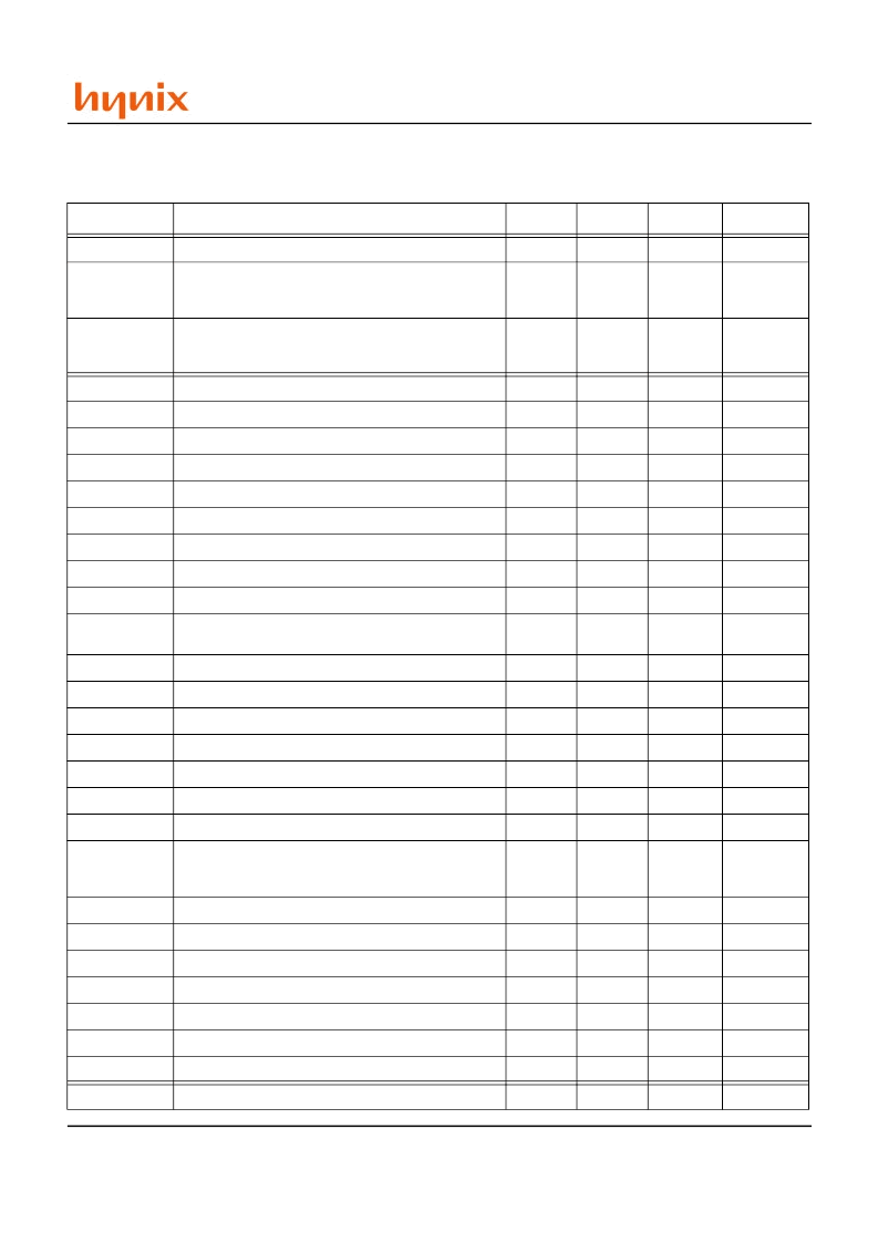
Rev.0.9 / Dec.2000
47
Direct RDRAM
256/288-Mbit (512Kx16/18x32s) Preliminary
Timing Conditions.
Table 18: Timing Conditions
Symbol
Parameter
Min
Max
Unit
Figure(s)
t
DCW
Domain crossing window
-0.1
0.1
t
CYCLE
Figure 60:
t
DR
, t
DF
DQA/DQB/ROW/COL input rise/fall times (20% to 80%)
Use the minimum value of these parameters during testing.
0.2
0.65
ns
Figure 55:
t
S
, t
H
DQA/DQB/ROW/COL-to-CFM setup/hold
@ t
CYCLE
=2.50ns/2.81ns/3.33ns
0.200
b
/0.240
b,c
/0.275
b,d
-
ns
Figure 55:
t
DR1,
t
DF1
SIO0, SIO1 input rise and fall times
-
5.0
ns
Figure 57:
t
DR2,
t
DF2
CMD, SCK input rise and fall times
-
2.0
ns
Figure 57:
t
CYCLE1
SCK cycle time - Serial control register transactions
1000
-
ns
Figure 57:
SCK cycle time - Power transitions
10
-
ns
Figure 57:
t
S1
CMD setup time to SCK rising or falling edge
e
1.25
-
ns
Figure 57:
t
H1
CMD hold time to SCK rising or falling edge
e
1
-
ns
Figure 57:
t
CH1
, t
CL1
SCK high and low times
4.25
-
ns
Figure 57:
t
S2
SIO0 setup time to SCK falling edge
40
-
ns
Figure 57:
t
H2
SIO0 hold time to SCK falling edge
40
-
ns
Figure 57:
t
S3
PDEV setup time on DQA5..0 to SCK rising edge.
0
-
ns
Figure 48:,
Figure 57:
t
H3
PDEV hold time on DQA5..0 to SCK rising edge.
5.5
-
ns
t
S4
ROW2..0, COL4..0 setup time for quiet window
-1
-
t
CYCLE
Figure 48:
t
CYCLE
CTM and CFM cycle times (-600)
3.33
3.83
ns
Figure 54:
CTM and CFM cycle times (-711)
2.80
3.83
ns
Figure 54:
CTM and CFM cycle times (-800)
2.50
3.83
ns
Figure 54:
t
CR
, t
CF
CTM and CFM input rise and fall times
0.2
0.5
ns
Figure 54:
t
CH
, t
CL
CTM and CFM high and low times
40%
60%
t
CYCLE
Figure 54:
t
TR
CTM-CFM differential (MSE/MS=0/0)
CTM-CFM differential (MSE/MS=1/1)
a
0.0
0.9
1.0
1.0
t
CYCLE
Figure 42:
Figure 54:
t
H4
ROW2..0, COL4..0 hold time for quiet window
f
5
-
t
CYCLE
Figure 48:
t
NPQ
Quiet on ROW/COL bits during NAP/PDN entry
4
-
t
CYCLE
Figure 47:
t
READTOCC
Offset between read data and CC packets (same device)
12
-
t
CYCLE
Figure 52:
t
CCSAMTOREAD
Offset between CC packet and read data (same device)
8
-
t
CYCLE
Figure 52:
t
CE
CTM/CFM stable before NAP/PDN exit
2
-
t
CYCLE
Figure 48:
t
CD
CTM/CFM stable after NAP/PDN entry
100
-
t
CYCLE
Figure 47:
t
FRM
ROW packet to COL packet ATTN framing delay
7
-
t
CYCLE
Figure 46:
相關(guān)PDF資料 |
PDF描述 |
|---|---|
| HY5V16CF | 1Mx16|3.3V|4K|H|SDR SDRAM - 16M |
| HY5V16CF-H | x16 SDRAM |
| HY5V16CF-S | x16 SDRAM |
| HY6116-10 | x8 SRAM |
| HY6116-12 | x8 SRAM |
相關(guān)代理商/技術(shù)參數(shù) |
參數(shù)描述 |
|---|---|
| HY5S2B6DLF-BE | 制造商:HYNIX 制造商全稱:Hynix Semiconductor 功能描述:4Banks x 2M x 16bits Synchronous DRAM |
| HY5S2B6DLFP-BE | 制造商:HYNIX 制造商全稱:Hynix Semiconductor 功能描述:4Banks x 2M x 16bits Synchronous DRAM |
| HY5S2B6DLFP-SE | 制造商:HYNIX 制造商全稱:Hynix Semiconductor 功能描述:4Banks x 2M x 16bits Synchronous DRAM |
| HY5S2B6DLF-SE | 制造商:HYNIX 制造商全稱:Hynix Semiconductor 功能描述:4Banks x 2M x 16bits Synchronous DRAM |
| HY5S5B2BLF-6E | 制造商:HYNIX 制造商全稱:Hynix Semiconductor 功能描述:256M (8Mx32bit) Mobile SDRAM |
發(fā)布緊急采購,3分鐘左右您將得到回復(fù)。