- 您現(xiàn)在的位置:買賣IC網 > PDF目錄223992 > HY27US081G1MSES (HYNIX SEMICONDUCTOR INC) 128M X 8 FLASH 2.7V PROM, 45 ns, PDSO48 PDF資料下載
參數(shù)資料
| 型號: | HY27US081G1MSES |
| 廠商: | HYNIX SEMICONDUCTOR INC |
| 元件分類: | PROM |
| 英文描述: | 128M X 8 FLASH 2.7V PROM, 45 ns, PDSO48 |
| 封裝: | 12 X 17 MM, 0.65 MM PITCH, USOP1-48 |
| 文件頁數(shù): | 37/39頁 |
| 文件大小: | 312K |
| 代理商: | HY27US081G1MSES |
第1頁第2頁第3頁第4頁第5頁第6頁第7頁第8頁第9頁第10頁第11頁第12頁第13頁第14頁第15頁第16頁第17頁第18頁第19頁第20頁第21頁第22頁第23頁第24頁第25頁第26頁第27頁第28頁第29頁第30頁第31頁第32頁第33頁第34頁第35頁第36頁當前第37頁第38頁第39頁
Rev 0.2 / May. 2007
7
Preliminary
HY27US(08/16)1G1M Series
1Gbit (128Mx8bit / 64Mx16bit) NAND Flash
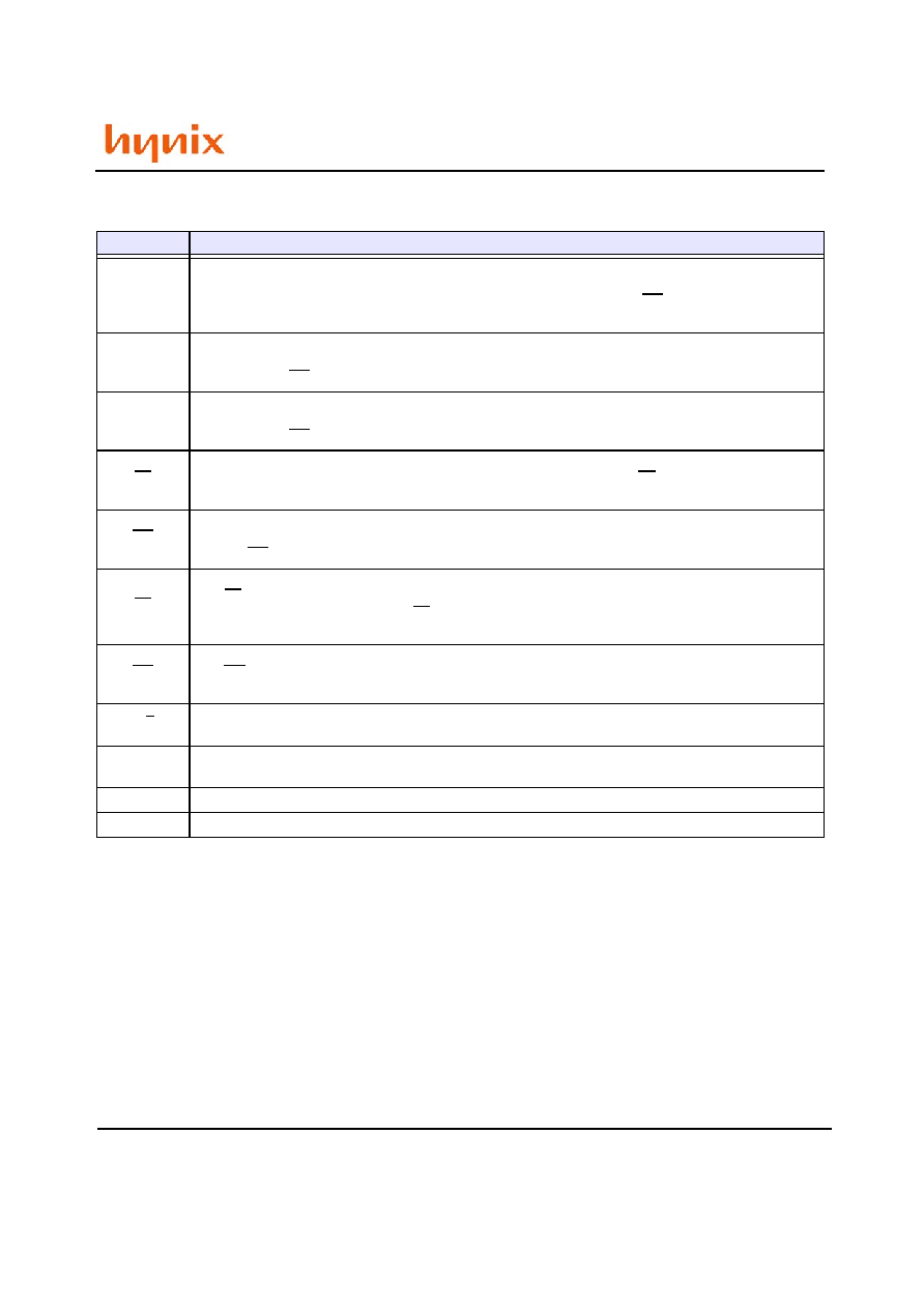
1.2 PIN DESCRIPTION
Pin Name
Description
IO0-IO7
IO8-IO15(1)
DATA INPUTS/OUTPUTS
The IO pins allow to input command, address and data and to output data during read / program
operations. The inputs are latched on the rising edge of Write Enable (WE). The I/O buffer float to
High-Z when the device is deselected or the outputs are disabled.
CLE
COMMAND LATCH ENABLE
This input activates the latching of the IO inputs inside the Command Register on the Rising edge of
Write Enable (WE).
ALE
ADDRESS LATCH ENABLE
This input activates the latching of the IO inputs inside the Address Register on the Rising edge of
Write Enable (WE).
CE
CHIP ENABLE
This input controls the selection of the device. When the device is busy CE low does not deselect the
memory.
WE
WRITE ENABLE
This input acts as clock to latch Command, Address and Data. The IO inputs are latched on the rise
edge of WE.
RE
READ ENABLE
The RE input is the serial data-out control, and when active drives the data onto the I/O bus. Data is
valid tREA after the falling edge of RE which also increments the internal column address counter by
one.
WP
WRITE PROTECT
The WP pin, when Low, provides an Hardware protection against undesired modify (program / erase)
operations.
R/B
READY BUSY
The Ready/Busy output is an Open Drain pin that signals the state of the memory.
VCC
SUPPLY VOLTAGE
The VCC supplies the power for all the operations (Read, Write, Erase).
VSS
GROUND
NC
NO CONNECTION
Table 2: Pin Description
NOTE:
1. For x16 version only
2. A 0.1uF capacitor should be connected between the Vcc Supply Voltage pin and the Vss Ground pin to decouple
the current surges from the power supply. The PCB track widths must be sufficient to carry the currents required
during program and erase operations.
相關PDF資料 |
PDF描述 |
|---|---|
| HY27US081G1MTCS | 128M X 8 FLASH 2.7V PROM, 45 ns, PDSO48 |
| HY27US081G1MTPMP | 128M X 8 FLASH 2.7V PROM, 45 ns, PDSO48 |
| HY5116100BJ-70 | 16M X 1 FAST PAGE DRAM, 70 ns, PDSO24 |
| HY5116804CSLT-80 | 2M X 8 EDO DRAM, 80 ns, PDSO28 |
| HY514400ALT-60 | 1M X 4 FAST PAGE DRAM, 60 ns, PDSO20 |
相關代理商/技術參數(shù) |
參數(shù)描述 |
|---|---|
| HY27US08281A | 制造商:HYNIX 制造商全稱:Hynix Semiconductor 功能描述:128Mbit (16Mx8bit / 8Mx16bit) NAND Flash Memory |
| HY27US08282A | 制造商:HYNIX 制造商全稱:Hynix Semiconductor 功能描述:128Mbit (16Mx8bit / 8Mx16bit) NAND Flash Memory |
| HY27US08561A | 制造商:HYNIX 制造商全稱:Hynix Semiconductor 功能描述:256Mbit (32Mx8bit / 16Mx16bit) NAND Flash |
| HY27US08561A-T (P) | 制造商:SK Hynix Inc 功能描述: |
| HY27US08561M | 制造商:HYNIX 制造商全稱:Hynix Semiconductor 功能描述:256Mbit (32Mx8bit / 16Mx16bit) NAND Flash |
發(fā)布緊急采購,3分鐘左右您將得到回復。