- 您現(xiàn)在的位置:買賣IC網(wǎng) > PDF目錄370474 > HD74AC (Hitachi,Ltd.) HD74AC Series Common Information PDF資料下載
參數(shù)資料
| 型號: | HD74AC |
| 廠商: | Hitachi,Ltd. |
| 英文描述: | HD74AC Series Common Information |
| 中文描述: | HD74AC系列通用信息 |
| 文件頁數(shù): | 5/52頁 |
| 文件大小: | 220K |
| 代理商: | HD74AC |
第1頁第2頁第3頁第4頁當(dāng)前第5頁第6頁第7頁第8頁第9頁第10頁第11頁第12頁第13頁第14頁第15頁第16頁第17頁第18頁第19頁第20頁第21頁第22頁第23頁第24頁第25頁第26頁第27頁第28頁第29頁第30頁第31頁第32頁第33頁第34頁第35頁第36頁第37頁第38頁第39頁第40頁第41頁第42頁第43頁第44頁第45頁第46頁第47頁第48頁第49頁第50頁第51頁第52頁
FACT Descriptions and Family Characteristics
4
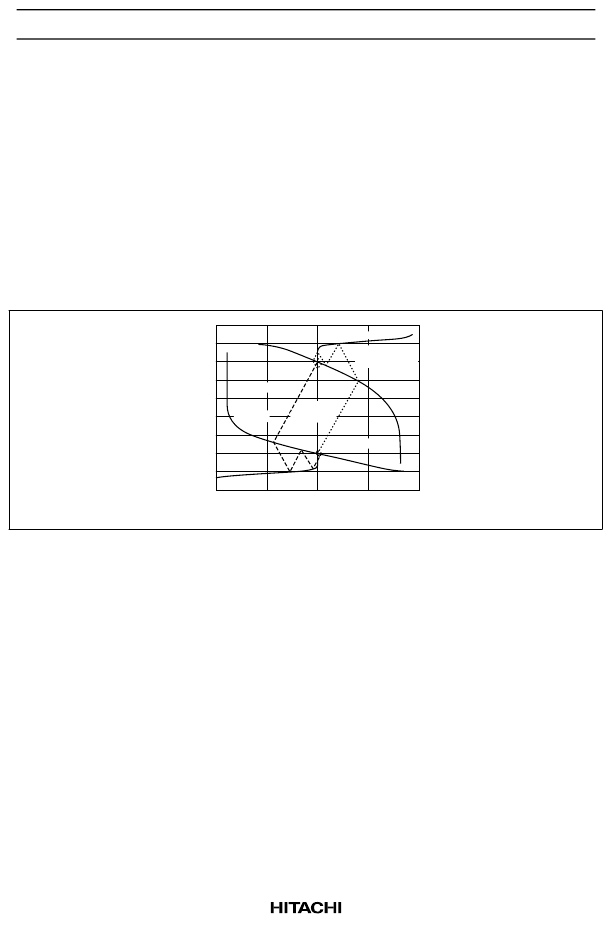
1.7.2 Dynamic Output Drive
Traditionally, in order to predict what incident wave voltages would occur in a system, the designer was
required to do an output analysis using a Bergeron diagram. Not only is this a long and time-consuming
operation, but the designer needed to depend upon the accuracy and reliability of the manufacturer-supplied
‘typical’ output I/V curve. Additionally, there was no way to guarantee that any supplied device would
meet these ‘typical’ performance values across the operating voltage and temperature limits. Hitachi has
taken the necessary steps to guarantee incident wave switching on transmission lines with impedances as
low as 50
.
Figure 2 shows a Bergerton diagram for switching both high-to-low and low-to-high. On the right side of
the graph (I
out
> 0), are the V
OH
and I
IH
curves for FACT logic while on the left side (I
out
< 0), are the curves
for V
OL
and I
IL
. Although we will only discuss here the low-to-high transition, the information presented
may be applied to a high-to-low transition.
0
Current (A)
0.1
0.2
–0.1
–0.2
–2
–1
0
1
2
3
4
5
6
7
V
V
OH
/I
OH
HIGH-to-LOW
LOW-to-HIGH
Line 1
Slope = 50
Line 2
Slope = 50
V
IN
/I
IN
V
OL
/I
OL
Figure 2 Gate Driving 50
Line Reflection Diagram
Begin analysis at the V
OL
(quiescent) point. This is the intersection of the V
OL
/I
OL
curve for the output and
the V
IN
/I
IN
curve for the input. For CMOS inputs and outputs, this point will be approximately 100 mV.
Then draw a 50
load line from this intersection to the V
OH
/I
OH
curve as shown by Line 1. This
intersection is the voltage that the incident wave will have. Here it occurs at approximately 3.95 V. Then
draw a line with a slope of –50
from this first intersection point to the V
IN
/I
IN
curve as shown by Line 2.
This second intersection will be the first reflection back from the input gate. Continue this process of
drawing the load line from each intersection to the next. Lines terminating on the V
OH
/I
OH
curve should
have positive slopes while lines terminating on the V
IN
/I
IN
curve should have negative slopes.
Each intersection point predicts the voltage of each reflected wave on the transmission line. Intersection
points on the V
OH
/I
OH
curve will be waves travelling from the driver to the receiver while intersection points
on the V
IN
/I
IN
curve will be waves travelling from the receiver to the driver.
Figure 3 and 4 show the resultant waveforms. Each division on the time scale represents the propagation
delay of the transmission line.
相關(guān)PDF資料 |
PDF描述 |
|---|---|
| HD74ALVC162244 | 16-bit Buffer / Driver with 3-state Outputs(帶三態(tài)輸出的16位緩沖器/驅(qū)動(dòng)器) |
| HD74ALVC162334 | 16-bit Universal Bus Driver with 3-state Outputs(帶三態(tài)輸出的16位通用總線驅(qū)動(dòng)器) |
| HD74ALVC16244 | 16-bit Buffer / Driver with 3-state Outputs(帶三態(tài)輸出的16位緩沖器/驅(qū)動(dòng)器) |
| HD74ALVC162831 | 1-bit to 4-bit Address Register / Driver with 3-state Outputs(三態(tài)輸出的1位-4位地址寄存器/驅(qū)動(dòng)器) |
| HD74ALVC162834A | 1-Of-8 Data Selectors/Multiplexers 16-CDIP -55 to 125 |
相關(guān)代理商/技術(shù)參數(shù) |
參數(shù)描述 |
|---|---|
| HD74AC00 | 制造商:HITACHI 制造商全稱:Hitachi Semiconductor 功能描述:Quad 2-Input NAND Gate |
| HD74AC00FP | 制造商:未知廠家 制造商全稱:未知廠家 功能描述:Quad 2-input NAND Gate |
| HD74AC00FPEL | 制造商:RENESAS 制造商全稱:Renesas Technology Corp 功能描述:Quad 2-Input NAND Gate |
| HD74AC00P | 制造商:RENESAS 制造商全稱:Renesas Technology Corp 功能描述:Quad 2-Input NAND Gate |
| HD74AC00RPEL | 制造商:RENESAS 制造商全稱:Renesas Technology Corp 功能描述:Quad 2-Input NAND Gate |
發(fā)布緊急采購,3分鐘左右您將得到回復(fù)。