- 您現(xiàn)在的位置:買賣IC網(wǎng) > PDF目錄295495 > DDC112U/1K (TEXAS INSTRUMENTS INC) 2-CH 20-BIT DELTA-SIGMA ADC, SERIAL ACCESS, PDSO28 PDF資料下載
參數(shù)資料
| 型號(hào): | DDC112U/1K |
| 廠商: | TEXAS INSTRUMENTS INC |
| 元件分類: | ADC |
| 英文描述: | 2-CH 20-BIT DELTA-SIGMA ADC, SERIAL ACCESS, PDSO28 |
| 封裝: | GREEN, PLASTIC, SOIC-28 |
| 文件頁數(shù): | 13/34頁 |
| 文件大?。?/td> | 776K |
| 代理商: | DDC112U/1K |
第1頁第2頁第3頁第4頁第5頁第6頁第7頁第8頁第9頁第10頁第11頁第12頁當(dāng)前第13頁第14頁第15頁第16頁第17頁第18頁第19頁第20頁第21頁第22頁第23頁第24頁第25頁第26頁第27頁第28頁第29頁第30頁第31頁第32頁第33頁第34頁
DDC112
20
SBAS085B
www.ti.com
SPECIAL CONSIDERATIONS
NCONT MODE INTEGRATION TIME
The DDC112 uses a relatively fast clock. For CLK = 10MHz,
this allows TINT to be adjusted in steps of 100ns since CONV
should be synchronized to CLK. However, for the internal
measurement, reset and auto-zero operations, a slower
clock is more efficient. The DDC112 divides CLK by six and
uses this slower clock with a period of 600ns to run the m/r/
az cycle and data ready logic.
Because of the divider, it is possible for the integration time
to be a non-integer number of slow clock periods. For
example, if TINT = 5000 CLK periods (500s for CLK = 10MHz),
there will be 833 1/3 slow clocks in an integration period. This
non-integer relationship between TINT and the slow clock
period causes the number of rising and falling slow clock
edges within an integration period to change from integration
to integration. The digital coupling of these edges to the
integrators will in turn change from integration to integration
which produces noise. The change in the clock edges is not
random, but will repeat every 3 integrations. The coupling
noise on the integrators appears as a tone with a frequency
equal to the rate at which the coupling repeats.
To avoid this problem in cont mode, the internal slow clock
is shut down after the m/r/az cycle is complete when it is no
longer needed. It starts up again just after the next integra-
tion begins. Since the slow clock is always off when CONV
toggles, the same number of slow clock edges fall within an
integration period regardless of its length. Therefore,
TINT ≥ 4794 CLK periods will not produce the coupling
problem described above.
For the ncont mode however, the slow clock must always be
left running. The m/r/az cycle is not completed before an
integration ends. It is then possible to have digital coupling to
the integrators. The digital coupling noise depends heavily on
the layout of the printed circuit board used for the DDC112.
For solid grounds and power supplies with good bypassing,
it is possible to greatly reduce the coupling. However, for
ensuring the best performance in the ncont mode, the inte-
gration time should be chosen to be an integer multiple of
1/(2fSLOWCLOCK). For CLK = 10MHz, the integration time
should be an integer multiple of 300ns—TINT = 100s is not.
A better choice would be TINT = 99s.
DATA READY
The DVALID signal which indicates that data is ready is
generated using the internal slow clock. The phase relation-
ship between this clock and CLK is set when power is first
applied and is random. Since CONV is synchronized with
CLK, it will have a random phase relationship with respect to
the slow clock. When TINT > t6, the slow clock will temporarily
shut down as described above. This shutdown process
synchronizes the internal clock with CONV so that the time
between when CONV toggles to when DVALID goes LOW
(t7 and t8) is fixed.
For TINT ≤ t6, the internal slow clock, is not allowed to shut
down and the synchronization never occurs. Therefore, the
time between CONV toggling and DVALID indicating data is
ready has uncertainty due to the random phase relationship
between CONV and the slow clock. This variation is
±1/(2f
SLOWCLOCK) or ±3/fCLK. The timing to the second DVALID
in the ncont mode will not have a variation since it is
triggered off the first data ready (t9) and both are derived
from the slow clock.
Polling DVALID to determine when data is ready eliminates
any concern about the variation in timing since the readback
is automatically adjusted as needed. If the data readback is
triggered off the toggling of CONV directly (instead of poll-
ing), then waiting the maximum value of t7 or t8 insures that
data will always be ready before readback occurs.
Data Retrieval
In the continuous and noncontinuous modes of operation,
the data from the last conversion is available for retrieval with
the falling edge of DVALID (see Figure 22). The falling edge
of DXMIT in combination with the data clock (DCLK) will
initiate the serial transmission of the data from the DDC112.
Typically, data is retrieved from the DDC112 as soon as
DVALID falls and completed before the next CONV transition
from HIGH to LOW or LOW to HIGH occurs. If this is not the
case, care should be taken to stop activity on DCLK and
consequently DOUT by at least 10
s around a CONV tran-
sition. If this caution is ignored it is possible that the integra-
tion that is being initiated by CONV will have additional noise
introduced.
The serial output data at DOUT is transmitted in Straight
Binary Code per Table VIII. An output offset has been built
into the DDC112 to allow for the measurement of input
signals near and below zero. Board leakage up to
≈ –0.4%
of the positive full-scale can be tolerated before the digital
output clips to all zeroes.
Cascading Multiple Converters
Multiple DDC112 units can be connected in serial or parallel
configurations, as illustrated in Figures 20 and 21.
DOUT can be used with DIN to
daisy-chain several DDC112
devices together to minimize wiring. In this mode of opera-
tion, the serial data output is shifted through multiple DDC112s,
as illustrated in Figure 20.
RPULLUP prevents DIN from floating when DXMIT is HIGH.
Care should be taken to keep the capacitive load on DOUT
as low as possible when running CLK=15MHz.
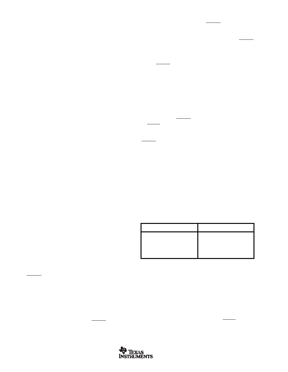
CODE
INPUT SIGNAL
1111 1111 1111 1111 1111
FS
1111 1111 1111 1111 1110
FS – 1LSB
0000 0001 0000 0000 0001
+1LSB
0000 0001 0000 0000 0000
Zero
0000 0000 0000 0000 0000
–0.4% FS
TABLE VIII. Straight Binary Code Table.
相關(guān)PDF資料 |
PDF描述 |
|---|---|
| DDC123JK-7-F | 100 mA, 50 V, 2 CHANNEL, NPN, Si, SMALL SIGNAL TRANSISTOR |
| DDL24W700G30LF | 24 CONTACT(S), FEMALE, D SUBMINIATURE CONNECTOR, SOLDER, SOCKET |
| DDV36W443G40LF | 36 CONTACT(S), FEMALE, D SUBMINIATURE CONNECTOR, SOLDER, SOCKET |
| DDV47W143G30LF | 47 CONTACT(S), FEMALE, D SUBMINIATURE CONNECTOR, SOLDER, SOCKET |
| DDV47W143H40LF | 47 CONTACT(S), FEMALE, D SUBMINIATURE CONNECTOR, SOLDER, SOCKET |
相關(guān)代理商/技術(shù)參數(shù) |
參數(shù)描述 |
|---|---|
| DDC112UG4 | 功能描述:模數(shù)轉(zhuǎn)換器 - ADC Dual Current Input 20-Bit RoHS:否 制造商:Texas Instruments 通道數(shù)量:2 結(jié)構(gòu):Sigma-Delta 轉(zhuǎn)換速率:125 SPs to 8 KSPs 分辨率:24 bit 輸入類型:Differential 信噪比:107 dB 接口類型:SPI 工作電源電壓:1.7 V to 3.6 V, 2.7 V to 5.25 V 最大工作溫度:+ 85 C 安裝風(fēng)格:SMD/SMT 封裝 / 箱體:VQFN-32 |
| DDC112UK | 功能描述:模數(shù)轉(zhuǎn)換器 - ADC Dual Current Input 20-Bit RoHS:否 制造商:Texas Instruments 通道數(shù)量:2 結(jié)構(gòu):Sigma-Delta 轉(zhuǎn)換速率:125 SPs to 8 KSPs 分辨率:24 bit 輸入類型:Differential 信噪比:107 dB 接口類型:SPI 工作電源電壓:1.7 V to 3.6 V, 2.7 V to 5.25 V 最大工作溫度:+ 85 C 安裝風(fēng)格:SMD/SMT 封裝 / 箱體:VQFN-32 |
| DDC112UK | 制造商:Texas Instruments 功能描述:DUAL CURRENT INPUT 20 BIT ANALOG/DIGITAL |
| DDC112UK | 制造商:Texas Instruments 功能描述:20BIT ADC DUAL SMD SOIC28 112 |
| DDC112UK/1K | 功能描述:模數(shù)轉(zhuǎn)換器 - ADC Dual Current Input 20-Bit RoHS:否 制造商:Texas Instruments 通道數(shù)量:2 結(jié)構(gòu):Sigma-Delta 轉(zhuǎn)換速率:125 SPs to 8 KSPs 分辨率:24 bit 輸入類型:Differential 信噪比:107 dB 接口類型:SPI 工作電源電壓:1.7 V to 3.6 V, 2.7 V to 5.25 V 最大工作溫度:+ 85 C 安裝風(fēng)格:SMD/SMT 封裝 / 箱體:VQFN-32 |
發(fā)布緊急采購,3分鐘左右您將得到回復(fù)。