- 您現(xiàn)在的位置:買賣IC網(wǎng) > PDF目錄4498 > APA150-FG144 (Microsemi SoC)IC FPGA PROASIC+ 150K 144-FBGA PDF資料下載
參數(shù)資料
| 型號: | APA150-FG144 |
| 廠商: | Microsemi SoC |
| 文件頁數(shù): | 149/178頁 |
| 文件大小: | 0K |
| 描述: | IC FPGA PROASIC+ 150K 144-FBGA |
| 標準包裝: | 160 |
| 系列: | ProASICPLUS |
| RAM 位總計: | 36864 |
| 輸入/輸出數(shù): | 100 |
| 門數(shù): | 150000 |
| 電源電壓: | 2.3 V ~ 2.7 V |
| 安裝類型: | 表面貼裝 |
| 工作溫度: | 0°C ~ 70°C |
| 封裝/外殼: | 144-LBGA |
| 供應商設備封裝: | 144-FPBGA(13x13) |
第1頁第2頁第3頁第4頁第5頁第6頁第7頁第8頁第9頁第10頁第11頁第12頁第13頁第14頁第15頁第16頁第17頁第18頁第19頁第20頁第21頁第22頁第23頁第24頁第25頁第26頁第27頁第28頁第29頁第30頁第31頁第32頁第33頁第34頁第35頁第36頁第37頁第38頁第39頁第40頁第41頁第42頁第43頁第44頁第45頁第46頁第47頁第48頁第49頁第50頁第51頁第52頁第53頁第54頁第55頁第56頁第57頁第58頁第59頁第60頁第61頁第62頁第63頁第64頁第65頁第66頁第67頁第68頁第69頁第70頁第71頁第72頁第73頁第74頁第75頁第76頁第77頁第78頁第79頁第80頁第81頁第82頁第83頁第84頁第85頁第86頁第87頁第88頁第89頁第90頁第91頁第92頁第93頁第94頁第95頁第96頁第97頁第98頁第99頁第100頁第101頁第102頁第103頁第104頁第105頁第106頁第107頁第108頁第109頁第110頁第111頁第112頁第113頁第114頁第115頁第116頁第117頁第118頁第119頁第120頁第121頁第122頁第123頁第124頁第125頁第126頁第127頁第128頁第129頁第130頁第131頁第132頁第133頁第134頁第135頁第136頁第137頁第138頁第139頁第140頁第141頁第142頁第143頁第144頁第145頁第146頁第147頁第148頁當前第149頁第150頁第151頁第152頁第153頁第154頁第155頁第156頁第157頁第158頁第159頁第160頁第161頁第162頁第163頁第164頁第165頁第166頁第167頁第168頁第169頁第170頁第171頁第172頁第173頁第174頁第175頁第176頁第177頁第178頁
ProASICPLUS Flash Family FPGAs
2- 62
v5.9
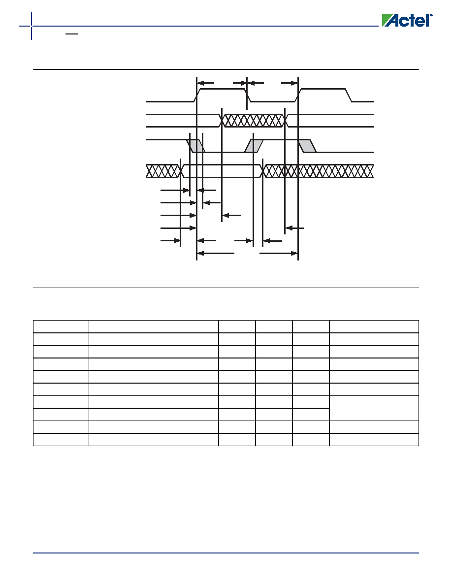
Asynchronous Write and Synchronous Read to the Same Location
Note: *New data is read if WB
↓ occurs before setup time. The stored data is read if WB ↓ occurs after hold time. The plot shows the
normal operation status.
Figure 2-35 Asynchronous Write and Synchronous Read to the Same Location
Table 2-59 TJ = 0°C to 110°C; VDD = 2.3 V to 2.7 V for Commercial/Industrial
TJ = –55°C to 150°C, VDD = 2.3 V to 2.7 V for Military/MIL-STD-883
Symbol txxx
Description
Min.
Max.
Units
Notes
CCYC
Cycle time
7.5
ns
CMH
Clock high phase
3.0
ns
CML
Clock low phase
3.0
ns
WBRCLKS
WB
↓ to RCLKS ↑ setup time
–0.1
ns
WBRCLKH
WB
↓ to RCLKS ↑ hold time
7.0
ns
OCH
Old DO valid from RCLKS
↑
3.0
ns
OCA/OCH
displayed
for
Access Timed Output
OCA
New DO valid from RCLKS
↑
7.5
ns
DWRRCLKS
DI to RCLKS
↑ setup time
0
ns
DWRH
DI to WB
↑ hold time
1.5
ns
Notes:
1. This behavior is valid for Access Timed Output and Pipelined Mode Output. The table shows the timings of an Access Timed Output.
2. In asynchronous write and synchronous read access to the same location, the new write data will be read out if the active write
signal edge occurs before or at the same time as the active read clock edge. If WB changes to low after hold time, the data will be
read.
3. A setup or hold time violation will result in unknown output data.
WB = {WRB + WBLKB}
RCLKS
DO
t
BRCLKH
New Data*
Last Cycle Data
t
WRCKS
t
OCH
t
OCA
DI
t
DWRRCLK
t
DWRH
t
CCYC
t
CMH
t
CML
相關PDF資料 |
PDF描述 |
|---|---|
| AMM25DRSD-S288 | CONN EDGECARD 50POS .156 EXTEND |
| RSA50DRMI | CONN EDGECARD 100POS .125 SQ WW |
| RMA50DRMI | CONN EDGECARD 100POS .125 SQ WW |
| HSM10DREF | CONN EDGECARD 20POS .156 EYELET |
| AMM24DRST | CONN EDGECARD 48POS DIP .156 SLD |
相關代理商/技術參數(shù) |
參數(shù)描述 |
|---|---|
| APA150-FG144A | 功能描述:IC FPGA PROASIC+ 150K 144-FBGA RoHS:否 類別:集成電路 (IC) >> 嵌入式 - FPGA(現(xiàn)場可編程門陣列) 系列:ProASICPLUS 標準包裝:90 系列:ProASIC3 LAB/CLB數(shù):- 邏輯元件/單元數(shù):- RAM 位總計:36864 輸入/輸出數(shù):157 門數(shù):250000 電源電壓:1.425 V ~ 1.575 V 安裝類型:表面貼裝 工作溫度:-40°C ~ 125°C 封裝/外殼:256-LBGA 供應商設備封裝:256-FPBGA(17x17) |
| APA150-FG144I | 功能描述:IC FPGA PROASIC+ 150K 144-FBGA RoHS:否 類別:集成電路 (IC) >> 嵌入式 - FPGA(現(xiàn)場可編程門陣列) 系列:ProASICPLUS 標準包裝:40 系列:SX-A LAB/CLB數(shù):6036 邏輯元件/單元數(shù):- RAM 位總計:- 輸入/輸出數(shù):360 門數(shù):108000 電源電壓:2.25 V ~ 5.25 V 安裝類型:表面貼裝 工作溫度:0°C ~ 70°C 封裝/外殼:484-BGA 供應商設備封裝:484-FPBGA(27X27) |
| APA150-FG256 | 功能描述:IC FPGA PROASIC+ 150K 256-FBGA RoHS:否 類別:集成電路 (IC) >> 嵌入式 - FPGA(現(xiàn)場可編程門陣列) 系列:ProASICPLUS 標準包裝:90 系列:ProASIC3 LAB/CLB數(shù):- 邏輯元件/單元數(shù):- RAM 位總計:36864 輸入/輸出數(shù):157 門數(shù):250000 電源電壓:1.425 V ~ 1.575 V 安裝類型:表面貼裝 工作溫度:-40°C ~ 125°C 封裝/外殼:256-LBGA 供應商設備封裝:256-FPBGA(17x17) |
| APA150-FG256A | 功能描述:IC FPGA PROASIC+ 150K 256-FBGA RoHS:否 類別:集成電路 (IC) >> 嵌入式 - FPGA(現(xiàn)場可編程門陣列) 系列:ProASICPLUS 標準包裝:90 系列:ProASIC3 LAB/CLB數(shù):- 邏輯元件/單元數(shù):- RAM 位總計:36864 輸入/輸出數(shù):157 門數(shù):250000 電源電壓:1.425 V ~ 1.575 V 安裝類型:表面貼裝 工作溫度:-40°C ~ 125°C 封裝/外殼:256-LBGA 供應商設備封裝:256-FPBGA(17x17) |
| APA150-FG256I | 功能描述:IC FPGA PROASIC+ 150K 256-FBGA RoHS:否 類別:集成電路 (IC) >> 嵌入式 - FPGA(現(xiàn)場可編程門陣列) 系列:ProASICPLUS 標準包裝:40 系列:SX-A LAB/CLB數(shù):6036 邏輯元件/單元數(shù):- RAM 位總計:- 輸入/輸出數(shù):360 門數(shù):108000 電源電壓:2.25 V ~ 5.25 V 安裝類型:表面貼裝 工作溫度:0°C ~ 70°C 封裝/外殼:484-BGA 供應商設備封裝:484-FPBGA(27X27) |
發(fā)布緊急采購,3分鐘左右您將得到回復。