- 您現(xiàn)在的位置:買賣IC網(wǎng) > PDF目錄375263 > ADS1250 20-Bit Data Acquisition System ANALOG-TO-DIGITAL CONVERTER PDF資料下載
參數(shù)資料
| 型號: | ADS1250 |
| 英文描述: | 20-Bit Data Acquisition System ANALOG-TO-DIGITAL CONVERTER |
| 中文描述: | 20位數(shù)據(jù)采集系統(tǒng)的模擬數(shù)字轉(zhuǎn)換器 |
| 文件頁數(shù): | 8/20頁 |
| 文件大小: | 196K |
| 代理商: | ADS1250 |
8
ADS1250
THEORY OF OPERATION
The ADS1250 is a precision, high dynamic range, 20-bit,
delta-sigma, A/D converter capable of achieving very high-
resolution digital results at high data rates. The analog input
signal is continuously sampled at a rate determined by the
frequency of the system clock (CLK). The sampled analog
input is modulated by the delta-sigma A/D modulator, fol-
lowed by a digital filter value. A programmable gain func-
tion is also incorporated in the delta-sigma modulator with
larger input sampling capacitors for higher gains. A sinc
5
digital low-pass filter processes the output of the delta-sigma
modulator and writes the result into the data output register.
The DRDY pin is pulled LOW indicating that new data is
available to be read by the external microcontroller/micro-
processor. As shown in the block diagram, the main func-
tional blocks of the ADS1250 are the programmable gain
amplifier, a fourth-order delta-sigma modulator, a digital
filter, control logic, and a serial interface. Each of these
functional blocks is described below.
ANALOG INPUT
The ADS1250 contains a fully differential analog input with
programmable gain. The fully differential switched capaci-
tor architecture provides low system noise, common-mode
rejection of 105dB, and excellent power supply rejection.
The selectable gains on the input are 1, 2, 4, or 8, which
gives a bipolar input voltage range from –4.096 to +4.096V,
to –512mV to +512mV, when the reference input voltage
equals +4.096V. The bipolar ranges are with respect to –V
IN
and not with respect to GND.
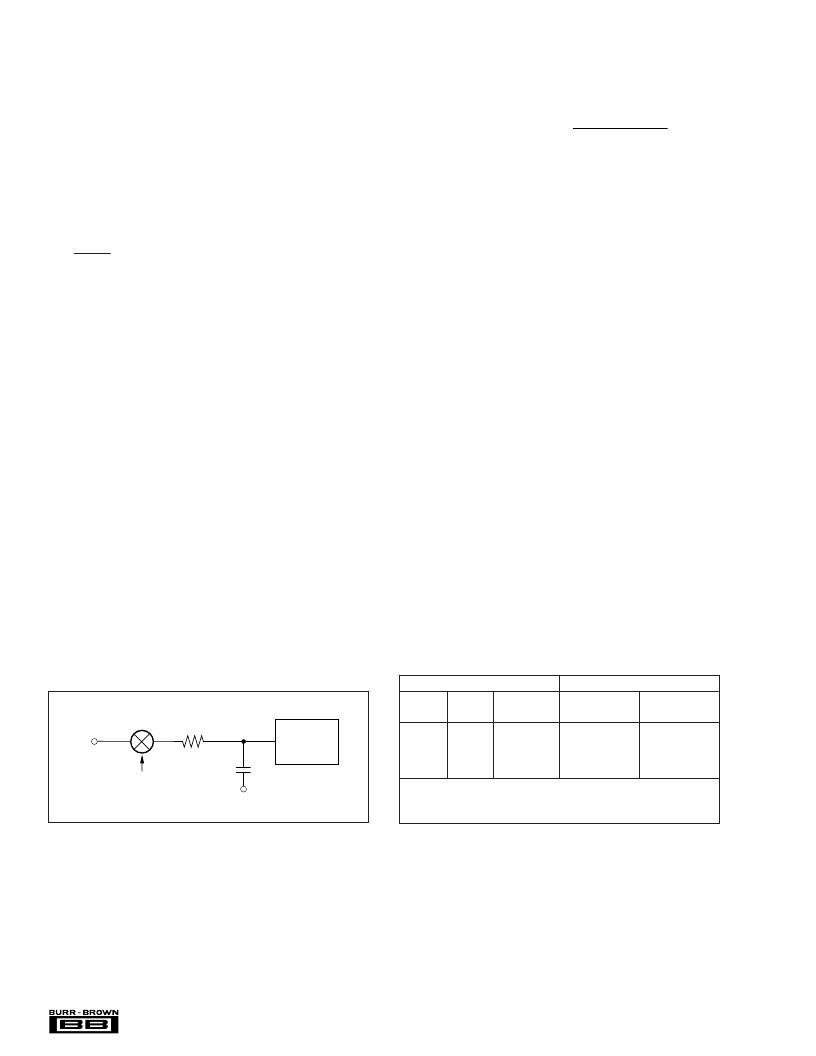
Figure 1 shows the basic input structure of the ADS1250.
The analog input impedance is directly related to the sam-
pling frequency of the input capacitor (f
MOD
), and the gain
setting (G) of the device. The sampling frequency of the
input capacitor is derived from the system clock (CLK).
Therefore, a lower CLK rate decreases the sampling fre-
quency, which results in a higher analog input impedance.
Additionally, a lower gain setting (G) decreases the sam-
pling capacitor size, which results in a higher analog input
impedance. This can be seen in the following equation:
A
Impedance ( )
9.6 MHz 104E3
CLK
G
IN
With regard to the analog input signal, the overall analog
performance of the device is affected by three items. First,
the input impedance can affect accuracy. If the source
impedance of the input signal is significant, or if there is
passive filtering prior to the ADS1250, a significant portion
of the signal can be lost across this external impedance. The
magnitude of the effect is dependent on the desired system
performance.
Second, the current into or out of the analog inputs must be
limited. Under no conditions should the current into or out
of the analog inputs exceed 10mA.
Third, to prevent aliasing of the input signal, the bandwidth
of the analog input signal must be band limited. The band-
width is a function of the system clock frequency. With a
system clock frequency of 9.6MHz, the data output rate is
25kHz, with a –3dB frequency of 5.4kHz. The –3dB fre-
quency scales with the system clock frequency.
To guarantee the best linearity of the ADS1250, a fully
differential signal is recommended.
PROGRAMMABLE GAIN AMPLIFIER
The PGA gain setting is programmed via the PGA pins on the
ADS1250. Changes in the gain setting (G) of the PGA results
in an increase in the input capacitor size. Therefore, higher
gain settings result in a lower analog input impedance.
The PGA of the ADS1250 can be set to a gain of 1, 2, 4, or
8, substantially increasing the dynamic range of the converter
and simplifying the interface to the more common transducers
(see Table I).
FIGURE 1. Analog Input Structure.
R
(1k
typical G)
Modulator Frequency
= f
MOD
Internal
Circuitry
C
(6pF typical G)
V
CM
A
IN
TABLE I. Full-Scale Range versus PGA Setting.
GAIN SETTING
ANALOG INPUT
DIFFERENTIAL
FSR (V)
SINGLE-ENDED
FSR (V)
G1
G0
GAIN VALUE
0
0
1
1
0
1
0
1
1
2
4
8
8.192
4.096
2.048
1.024
4.096
2.048
1.024
0.512
NOTE: Based on a 4.096V reference. The ADS1250 allows common-
mode voltage as long as the absolute input voltage on +V
IN
or –V
IN
does
not go below AGND or above +V
S
.
相關(guān)PDF資料 |
PDF描述 |
|---|---|
| ADS1250U | 20-Bit Data Acquisition System ANALOG-TO-DIGITAL CONVERTER |
| ADS1252 | 24-Bit, 40kHz ANALOG-TO-DIGITAL CONVERTER |
| ADS1252U | 24-Bit, 40kHz ANALOG-TO-DIGITAL CONVERTER |
| ADS1252K5 | 24-Bit, 20kHz, Low-Power ANALOG-TO-DIGITAL CONVERTER |
| ADS1254 | 24-Bit, 20kHz, Low Power ANALOG-TO-DIGITAL CONVERTER |
相關(guān)代理商/技術(shù)參數(shù) |
參數(shù)描述 |
|---|---|
| ADS1250U | 功能描述:模數(shù)轉(zhuǎn)換器 - ADC SpeedPlus 20-Bit Data Acq System RoHS:否 制造商:Texas Instruments 通道數(shù)量:2 結(jié)構(gòu):Sigma-Delta 轉(zhuǎn)換速率:125 SPs to 8 KSPs 分辨率:24 bit 輸入類型:Differential 信噪比:107 dB 接口類型:SPI 工作電源電壓:1.7 V to 3.6 V, 2.7 V to 5.25 V 最大工作溫度:+ 85 C 安裝風格:SMD/SMT 封裝 / 箱體:VQFN-32 |
| ADS1250U/1K | 功能描述:模數(shù)轉(zhuǎn)換器 - ADC SpeedPlus 20-Bit Data Acq System RoHS:否 制造商:Texas Instruments 通道數(shù)量:2 結(jié)構(gòu):Sigma-Delta 轉(zhuǎn)換速率:125 SPs to 8 KSPs 分辨率:24 bit 輸入類型:Differential 信噪比:107 dB 接口類型:SPI 工作電源電壓:1.7 V to 3.6 V, 2.7 V to 5.25 V 最大工作溫度:+ 85 C 安裝風格:SMD/SMT 封裝 / 箱體:VQFN-32 |
| ADS1250U/1KG4 | 功能描述:模數(shù)轉(zhuǎn)換器 - ADC SpeedPlus 20-Bit Data Acq System RoHS:否 制造商:Texas Instruments 通道數(shù)量:2 結(jié)構(gòu):Sigma-Delta 轉(zhuǎn)換速率:125 SPs to 8 KSPs 分辨率:24 bit 輸入類型:Differential 信噪比:107 dB 接口類型:SPI 工作電源電壓:1.7 V to 3.6 V, 2.7 V to 5.25 V 最大工作溫度:+ 85 C 安裝風格:SMD/SMT 封裝 / 箱體:VQFN-32 |
| ADS1250UG4 | 功能描述:模數(shù)轉(zhuǎn)換器 - ADC SpeedPlus 20-Bit Data Acq System RoHS:否 制造商:Texas Instruments 通道數(shù)量:2 結(jié)構(gòu):Sigma-Delta 轉(zhuǎn)換速率:125 SPs to 8 KSPs 分辨率:24 bit 輸入類型:Differential 信噪比:107 dB 接口類型:SPI 工作電源電壓:1.7 V to 3.6 V, 2.7 V to 5.25 V 最大工作溫度:+ 85 C 安裝風格:SMD/SMT 封裝 / 箱體:VQFN-32 |
| ADS1251 | 制造商:TI 制造商全稱:Texas Instruments 功能描述:24-Bit, 20kHz, Low-Power ANALOG-TO-DIGITAL CONVERTER |
發(fā)布緊急采購,3分鐘左右您將得到回復(fù)。