- 您現(xiàn)在的位置:買賣IC網(wǎng) > PDF目錄373980 > ADE7758 (Analog Devices, Inc.) Poly Phase Multifunction Energy Metering IC with Per Phase Information PDF資料下載
參數(shù)資料
| 型號: | ADE7758 |
| 廠商: | Analog Devices, Inc. |
| 英文描述: | Poly Phase Multifunction Energy Metering IC with Per Phase Information |
| 中文描述: | 多相多功能電能計量IC每相位信息 |
| 文件頁數(shù): | 56/68頁 |
| 文件大小: | 1584K |
| 代理商: | ADE7758 |
第1頁第2頁第3頁第4頁第5頁第6頁第7頁第8頁第9頁第10頁第11頁第12頁第13頁第14頁第15頁第16頁第17頁第18頁第19頁第20頁第21頁第22頁第23頁第24頁第25頁第26頁第27頁第28頁第29頁第30頁第31頁第32頁第33頁第34頁第35頁第36頁第37頁第38頁第39頁第40頁第41頁第42頁第43頁第44頁第45頁第46頁第47頁第48頁第49頁第50頁第51頁第52頁第53頁第54頁第55頁當(dāng)前第56頁第57頁第58頁第59頁第60頁第61頁第62頁第63頁第64頁第65頁第66頁第67頁第68頁
ADE7758
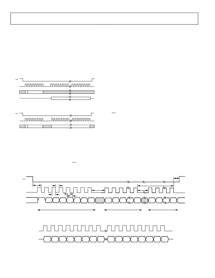
The communications register is an 8-bit write-only register. The
MSB determines whether the next data transfer operation is a
read or a write. The seven LSBs contain the address of the register
to be accessed. See Table 12 for a more detailed description.
Rev. A | Page 56 of 68
Figure 89 and Figure 90 show the data transfer sequences for a
read and write operation, respectively.
On completion of a data transfer (read or write), the ADE7758
once again enters into communications mode, i.e., the next
instruction followed must be a write to the communications
register.
0
MULTIBYTE
COMMUNICATIONS REGISTER WRITE
ADDRESS
0
DIN
SCLK
DOUT
READ DATA
CS
Figure 89. Reading Data from the ADE7758 via the Serial Interface
0
COMMUNICATIONS REGISTER WRITE
ADDRESS
1
DIN
SCLK
CS
MULTIBYTE
READ DATA
Figure 90. Writing Data to the ADE7758 via the Serial Interface
A data transfer is completed when the LSB of the ADE7758
register being addressed (for a write or a read) is transferred to
or from the ADE7758.
ADE7758 SERIAL WRITE OPERATION
The serial write sequence takes place as follows. With the
ADE7758 in communications mode and the CS input logic low,
a write to the communications register takes place first. The
MSB of this byte transfer must be set to 1, indicating that the
next data transfer operation is a write to the register. The seven
LSBs of this byte contain the address of the register to be written
to. The ADE7758 starts shifting in the register data on the next
falling edge of SCLK. All remaining bits of register data are
shifted in on the falling edge of the subsequent SCLK pulses
(see Figure 91).
As explained earlier, the data write is initiated by a write to the
communications register followed by the data. During a data
write operation to the ADE7758, data is transferred to all on-
chip registers one byte at a time. After a byte is transferred into
the serial port, there is a finite time duration before the content
in the serial port buffer is transferred to one of the ADE7758
on-chip registers. Although another byte transfer to the serial
port can start while the previous byte is being transferred to the
destination register, this second-byte transfer should not finish
until at least 900 ns after the end of the previous byte transfer.
This functionality is expressed in the timing specification t
6
(see
Figure 91). If a write operation is aborted during a byte transfer
(CS brought high), then that byte is not written to the
destination register.
Destination registers may be up to 3 bytes wide (see the
Accessing the ADE7758 On-Chip Registers section). Therefore,
the first byte shifted into the serial port at DIN is transferred to
the most significant byte (MSB) of the destination register. If
the destination register is 12 bits wide, for example, a two-byte
data transfer must take place. The data is always assumed to be
right justified; therefore, in this case, the four MSBs of the first
byte would be ignored and the four LSBs of the first byte written
to the ADE7758 would be the four MSBs of the 12-bit word.
Figure 92 illustrates this example.
0
DIN
SCLK
CS
t
2
t
3
t
1
t
4
t
5
t
7
t
6
t
8
COMMAND BYTE
MOST SIGNIFICANT BYTE
LEAST SIGNIFICANT BYTE
1
A6
A4
A5
A3
A2
A1
A0
DB7
DB0
DB7
DB0
t
7
Figure 91. Serial Interface Write Timing Diagram
0
SCLK
DIN
X
X
X
X
DB11
DB10
DB9
DB8
DB7
DB6
DB5
DB4
DB3
DB2
DB1
DB0
MOST SIGNIFICANT BYTE
LEAST SIGNIFICANT BYTE
Figure 92. 12-Bit Serial Write Operation
相關(guān)PDF資料 |
PDF描述 |
|---|---|
| ADE7758ARW | Poly Phase Multifunction Energy Metering IC with Per Phase Information |
| ADE7758ARWRL | Poly Phase Multifunction Energy Metering IC with Per Phase Information |
| ADE7758ARWZ | Poly Phase Multifunction Energy Metering IC with Per Phase Information |
| ADE7758ARWZRL | Poly Phase Multifunction Energy Metering IC with Per Phase Information |
| ADE7759ARSRL | Active Energy Metering IC with di/dt Sensor Interface |
相關(guān)代理商/技術(shù)參數(shù) |
參數(shù)描述 |
|---|---|
| ADE7758ARW | 制造商:Analog Devices 功能描述:Energy Measurement 24-Pin SOIC W 制造商:Analog Devices 功能描述:IC ENERGY METER |
| ADE7758ARWRL | 制造商:Analog Devices 功能描述:Energy Measurement 24-Pin SOIC W T/R 制造商:Analog Devices 功能描述:IC ENERGY METER |
| ADE7758ARWZ | 功能描述:IC ENERGY METERING 3PHASE 24SOIC RoHS:是 類別:集成電路 (IC) >> PMIC - 能量測量 系列:- 產(chǎn)品培訓(xùn)模塊:Lead (SnPb) Finish for COTS Obsolescence Mitigation Program 標(biāo)準(zhǔn)包裝:2,500 系列:* |
| ADE7758ARWZ | 制造商:Analog Devices 功能描述:ENERGY METERING IC 制造商:Analog Devices 功能描述:IC, POLY-PHASE ENERGY METERING, SOIC-24 |
| ADE7758ARWZ | 制造商:Analog Devices 功能描述:IC ENERGY METER 3 PHASE SOIC-24 |
發(fā)布緊急采購,3分鐘左右您將得到回復(fù)。