- 您現(xiàn)在的位置:買賣IC網(wǎng) > PDF目錄373980 > ADE7754ARRL (ANALOG DEVICES INC) ADE7754 PDF資料下載
參數(shù)資料
| 型號: | ADE7754ARRL |
| 廠商: | ANALOG DEVICES INC |
| 元件分類: | 模擬信號調(diào)理 |
| 英文描述: | ADE7754 |
| 中文描述: | SPECIALTY ANALOG CIRCUIT, PDSO24 |
| 封裝: | MS-013AD, SOIC-24 |
| 文件頁數(shù): | 31/44頁 |
| 文件大?。?/td> | 630K |
| 代理商: | ADE7754ARRL |
第1頁第2頁第3頁第4頁第5頁第6頁第7頁第8頁第9頁第10頁第11頁第12頁第13頁第14頁第15頁第16頁第17頁第18頁第19頁第20頁第21頁第22頁第23頁第24頁第25頁第26頁第27頁第28頁第29頁第30頁當(dāng)前第31頁第32頁第33頁第34頁第35頁第36頁第37頁第38頁第39頁第40頁第41頁第42頁第43頁第44頁
REV. PrG 01/03
PRELIMINARY TECHNICAL DATA
ADE7754
–
31
–
ADE7754 SERIAL INTERFACE
ADE7754 has a built-in SPI interface. The Serial Interface
of the ADE7754 is made of four signals SCLK, DIN,
DOUT and
CS
. The serial clock for a data transfer is applied
at the SCLK logic input. This logic input has a Schmidt-
trigger input structure, which allows slow rising (and falling)
clock edges to be used. All data transfer operations are
synchronized to the serial clock. Data is shifted into the
ADE7754 at the DIN logic input on the falling edge of
SCLK. Data is shifted out of the ADE7754 at the DOUT
logic output on a rising edge of SCLK. The
CS
logic input
is the chip select input. This input is used when multiple
devices share the serial bus. A falling edge on
CS
also resets
the serial interface and places the ADE7754 in communica-
tions mode. The
CS
input should be driven low for the entire
data transfer operation. Bringing
CS
high during a data
transfer operation will abort the transfer and place the serial
bus in a high impedance state. The
CS
logic input may be tied
low if the ADE7754 is the only device on the serial bus.
However with
CS
tied low, all initiated data transfer opera-
tions must be fully completed, i.e., the LSB of each register
must be transferred as there is no other way of bringing the
ADE7754 back into communications mode without resetting
the entire device, i.e., setting the
RESET
pin logic low.
All the ADE7754 functionality is accessible via several on-
chip registers
–
see Figure 39. The contents of these registers
can be updated or read using the on-chip serial interface.
After power-on or toggling the
RESET
pin low or a falling
edge on
CS
, the ADE7754 is placed in communications
mode. In communications mode the ADE7754 expects the
first communication to be a write to the internal Communi-
cations register. The data written to the Communications
register contains the address and specifies the next data
transfer to be a read or a write command. Therefore all data
transfer operations with the ADE7754, whether a read or a
write, must begin with a write to the Communications
register.
COMMUNICATIONS REGISTER
REGISTER # 1
REGISTER # 2
REGISTER # 3
REGISTER # n-1
REGISTER # n
IN
OUT
R
D
DIN
DOUT
IN
OUT
IN
OUT
IN
OUT
IN
OUT
Figure 39
–
Addressing ADE7754 Registers via the
Communications Register
The Communications register is an eight bit write only
register. The MSB determines whether the next data transfer
operation is a read or a write. The 6 LSBs contain the address
of the register to be accessed. See
ADE7754 Communications
Register
for a more detailed description.
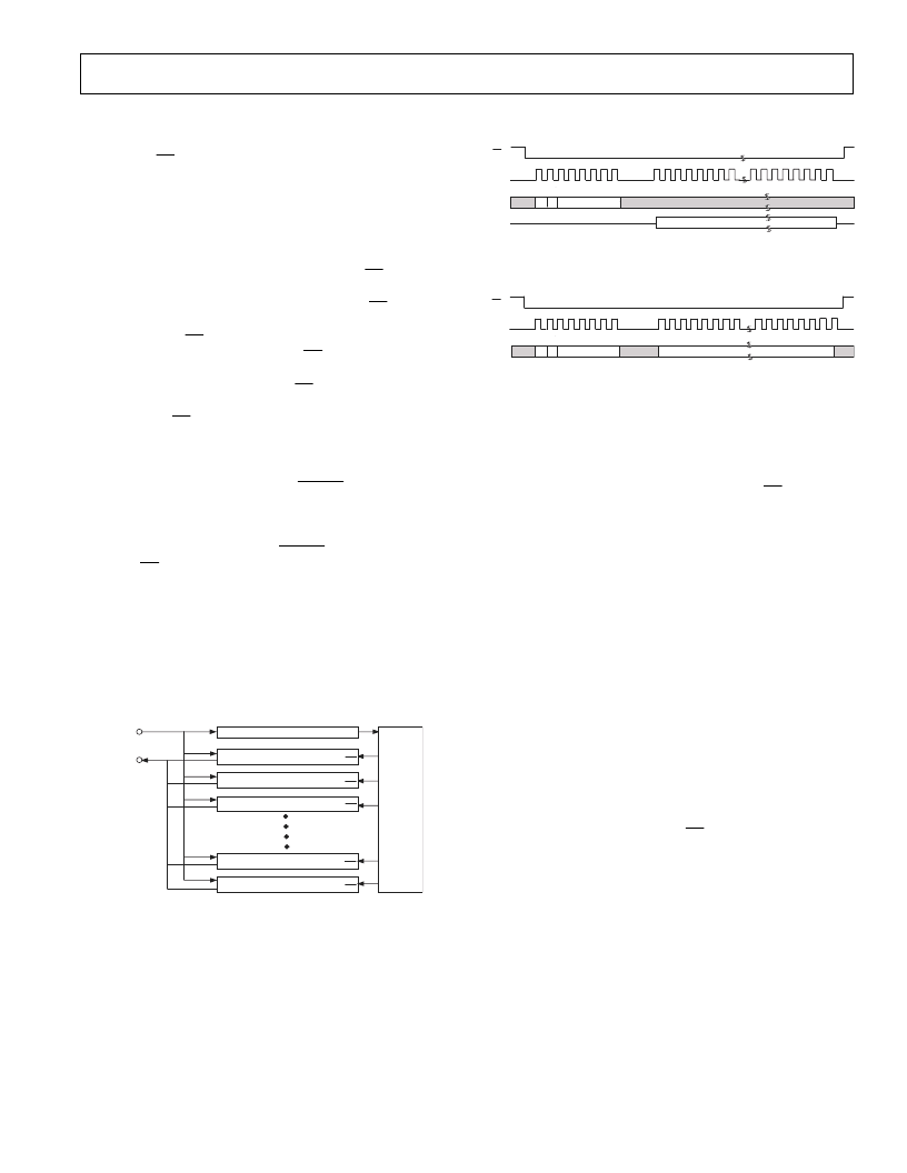
Figure 40 and Figure 41 show the data transfer sequences for
a read and write operation respectively.
On completion of a data transfer (read or write) the ADE7754
once again enters communications mode, i.e. the next in-
struction followed must be a write to the Communications
register.
COMMUNICATIONS REGISTER WRITE
0 0
ADDRESS
CS
DIN
DOUT
SCLK
MULTIBYTE READ DATA
Figure 40
–
Reading data from the ADE7754 via the
serial interface
COMMUNICATIONS REGISTER WRITE
1 0
ADDRESS
CS
DIN
SCLK
MULTIBYTE WRITE DATA
Figure 41
–
Writing data to the ADE7754 via the
serial interface
A data transfer is completed when the LSB of the ADE7754
register being addressed (for a write or a read) is transferred
to or from the ADE7754.
ADE7754 Serial Write Operation
The serial write sequence takes place as follows: with the
ADE7754 in communications mode and the
CS
input logic
low, a write to the communications register first takes place.
The MSB of this byte transfer must be set to 1, indicating that
the next data transfer operation is a write to the register. The
six LSBs of this byte contain the address of the register to be
written to. The ADE7754 starts shifting in the register data
on the next falling edge of SCLK. All remaining bits of
register data are shifted in on the falling edge of subsequent
SCLK pulses
–
see Figure 42.
As explained earlier the data write is initiated by a write to the
Communications register followed by the data. During a data
write operation to the ADE7754, data is transferred to all on-
chip registers one byte at a time. After a byte is transferred
into the serial port, there is a finite time duration before the
content in the serial port buffer is transferred to one of the
ADE7754 on-chip registers. Although another byte transfer
to the serial port can start while the previous byte is being
transferred to the destination register, this second byte
transfer should not finish until at least TBD after the end of
the previous byte transfer. This functionality is expressed in
the timing specification t
6
- see Figure 42. If a write operation
is aborted during a byte transfer (
CS
brought high), then that
byte will not be written to the destination register.
Destination registers may be up to 3 bytes wide
–
see
ADE7754 Register Descriptions
. Hence the first byte shifted
into the serial port at DIN is transferred to the MSB (Most
significant Byte) of the destination register. If the destination
register is 12 bits wide, for example, a two-byte data transfer
must take place. The data is always assumed to be right
justified, therefore in this case, the four MSBs of the first byte
would be ignored and the 4 LSBs of the first byte written to
the ADE7754 would be the 4MSBs of the 12-bit word.
Figure 43 illustrates this example.
相關(guān)PDF資料 |
PDF描述 |
|---|---|
| ADE7755AN-REF | Energy Metering IC with Pulse Output |
| ADE7755ARSRL | Energy Metering IC with Pulse Output |
| ADE7755 | Energy Metering IC with Pulse Output |
| ADE7755ARS | Energy Metering IC with Pulse Output |
| ADE7756EB | Evaluation Board Documentation AD7756 Energy metering IC |
相關(guān)代理商/技術(shù)參數(shù) |
參數(shù)描述 |
|---|---|
| ADE7754ARZ | 功能描述:IC ENERGY METERING 3PHASE 24SOIC RoHS:是 類別:集成電路 (IC) >> PMIC - 能量測量 系列:- 產(chǎn)品培訓(xùn)模塊:Lead (SnPb) Finish for COTS Obsolescence Mitigation Program 標(biāo)準(zhǔn)包裝:2,500 系列:* |
| ADE7754ARZRL | 功能描述:IC ENERGY METERING 3PHASE 24SOIC RoHS:是 類別:集成電路 (IC) >> PMIC - 能量測量 系列:- 產(chǎn)品培訓(xùn)模塊:Lead (SnPb) Finish for COTS Obsolescence Mitigation Program 標(biāo)準(zhǔn)包裝:2,500 系列:* |
| ADE7755 | 制造商:AD 制造商全稱:Analog Devices 功能描述:Energy Metering IC with Pulse Output |
| ADE7755AARSRL | 制造商:Analog Devices 功能描述:ENERGY METERING IC WITH P - Tape and Reel |
| ADE7755AN | 制造商:Rochester Electronics LLC 功能描述: 制造商:Analog Devices 功能描述: |
發(fā)布緊急采購,3分鐘左右您將得到回復(fù)。