- 您現(xiàn)在的位置:買賣IC網(wǎng) > PDF目錄157283 > 5962R9572201VQC (INTERSIL CORP) 16-BIT, 5 MHz, MICROPROCESSOR, CDIP40 PDF資料下載
參數(shù)資料
| 型號: | 5962R9572201VQC |
| 廠商: | INTERSIL CORP |
| 元件分類: | 微控制器/微處理器 |
| 英文描述: | 16-BIT, 5 MHz, MICROPROCESSOR, CDIP40 |
| 封裝: | CERAMIC, DIP-40 |
| 文件頁數(shù): | 27/29頁 |
| 文件大小: | 322K |
| 代理商: | 5962R9572201VQC |
第1頁第2頁第3頁第4頁第5頁第6頁第7頁第8頁第9頁第10頁第11頁第12頁第13頁第14頁第15頁第16頁第17頁第18頁第19頁第20頁第21頁第22頁第23頁第24頁第25頁第26頁當前第27頁第28頁第29頁
7
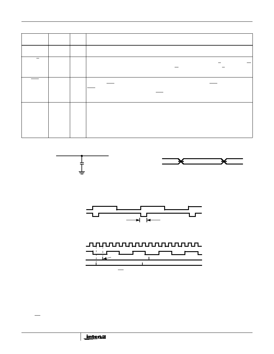
AC Test Circuit
NOTE: Includes stray and jig capacitance.
AC Testing Input, Output Waveform
NOTE: All inputs signals (other than CLK) must switch between VIL
Max -0.4V and VIH Min +0.4. CLK must switch between 0.4V and
VDD -0.4V. TR and TF must be less than or equal to 15ns. CLK TR
and TF must be less than or equal to 10ns.
ALE
25
O
ADDRESS LATCH ENABLE: is provided by the processor to latch the address into the 82C82 latch. It is
a HIGH pulse active during clock LOW of T1 of any bus cycle. Note that ALE is never oated.
DT/R
27
O
DATA TRANSMIT/RECEIVE: is needed in a minimum system that desires to use a data bus transceiver.
It is used to control the direction of data ow through the transceiver. Logically, DT/R is equivalent to S1
in maximum mode, and its timing is the same as for M/IO (T = HlGH, R = LOW). DT/R is held to a high
impedance logic one during local bus “hold acknowledge”.
DEN
26
O
DATA ENABLE: provided as an output enable for a bus transceiver in a minimum system which uses the
transceiver. DEN is active LOW during each memory and I/O access and for INTA cycles. For a read or
INTA cycle it is active from the middle of T2 until the middle of T4, while for a write cycle it is active from
the beginning of T2 until the middle of T4. DEN is held to a high impedance logic one during local bus
“hold acknowledge”.
HOLD
HLDA
31
30
I
O
HOLD: indicates that another master is requesting a local bus “hold”. To be a acknowledged, HOLD must
be active HIGH. The processor receiving the “hold” will issue a “hold acknowledge” (HLDA) in the middle
of a T4 or T1 clock cycle. Simultaneously with the issuance of HLDA, the processor will oat the local bus
and control lines. After HOLD is detected as being LOW, the processor will lower HLDA, and when the
processor needs to run another cycle, it will again drive the local bus and control lines.
HOLD is not an asynchronous input. External synchronization should be provided if the system cannot
otherwise guarantee the setup time.
Pin Descriptions (Continued)
SYMBOL
PIN
NUMBER
TYPE
DESCRIPTION
OUTPUT FROM
DEVICE UNDER TEST
TEST POINT
CL (NOTE)
INPUT
VIH
VIL - 0.4V
OUTPUT
VOH
1.5V
Timing Diagrams
READY TIMING AS COMPARED TO F5
RESET, NMI, AND MN/MX TIMING AS COMPARED TO F14 AND F16
NOTES:
4. F0 = 100kHz, 50% duty cycle square wave.
F1 = F0/2, F2 = F1/2 . . . F16 = F15/2.
5. READY, RESET, and NMI timing are as shown: T = 10
s.
6. All signals have rise/fall time limits: 100ns < t-rise, t-fall < 500ns.
7. RESET has a pulse width = 8T and occurs every two cycles of F16.
8. NMI has a pulse width = 4T and occurs every two cycles of F16.
9. MN/MX is a 50% duty cycle square wave and changes every eight cycles of F16.
4T
F5
READY
F14
RESET
F16
NMI
PULSE
HS-80C86RH
相關(guān)PDF資料 |
PDF描述 |
|---|---|
| 5962R9662801VYX | 4000/14000/40000 SERIES, ASYN NEGATIVE EDGE TRIGGERED 14-BIT UP BINARY COUNTER, CDFP16 |
| 59630-1-T-03-D | MAGNETIC FIELD SENSOR-HALL EFFECT, ROUND |
| 59630-1-T-03-F | MAGNETIC FIELD SENSOR-HALL EFFECT, ROUND |
| 59630-1-T-05-A | MAGNETIC FIELD SENSOR-HALL EFFECT, ROUND |
| 59630-1-T-05-F | MAGNETIC FIELD SENSOR-HALL EFFECT, ROUND |
相關(guān)代理商/技術(shù)參數(shù) |
參數(shù)描述 |
|---|---|
| 5962R9572701VXC | 制造商:Harris Corporation 功能描述: |
| 5962R9575701VXC | 制造商:Intersil Corporation 功能描述:Counter, Up/Down, 4 Bit Binary, 16 Pin, Ceramic, Flat Pack |
| 5962R9578201VCC | 制造商:Harris Corporation 功能描述: |
| 5962R9581401VXC | 制造商:Harris Corporation 功能描述: |
| 5962R9583301VFA | 功能描述:LVDS 接口集成電路 RoHS:否 制造商:Texas Instruments 激勵器數(shù)量:4 接收機數(shù)量:4 數(shù)據(jù)速率:155.5 Mbps 工作電源電壓:5 V 最大功率耗散:1025 mW 最大工作溫度:+ 85 C 封裝 / 箱體:SOIC-16 Narrow 封裝:Reel |
發(fā)布緊急采購,3分鐘左右您將得到回復(fù)。