- 您現(xiàn)在的位置:買賣IC網(wǎng) > PDF目錄375012 > XCR3320 (Xilinx, Inc.) 320 Macrocell SRAM CPLD(320宏單元靜態(tài)RAM復(fù)雜可編程邏輯器件) PDF資料下載
參數(shù)資料
| 型號: | XCR3320 |
| 廠商: | Xilinx, Inc. |
| 英文描述: | 320 Macrocell SRAM CPLD(320宏單元靜態(tài)RAM復(fù)雜可編程邏輯器件) |
| 中文描述: | 320宏單元CPLD實現(xiàn)的SRAM(320宏單元靜態(tài)RAM的復(fù)雜可編程邏輯器件) |
| 文件頁數(shù): | 2/43頁 |
| 文件大小: | 392K |
| 代理商: | XCR3320 |
第1頁當前第2頁第3頁第4頁第5頁第6頁第7頁第8頁第9頁第10頁第11頁第12頁第13頁第14頁第15頁第16頁第17頁第18頁第19頁第20頁第21頁第22頁第23頁第24頁第25頁第26頁第27頁第28頁第29頁第30頁第31頁第32頁第33頁第34頁第35頁第36頁第37頁第38頁第39頁第40頁第41頁第42頁第43頁
R
XCR3320: 320 Macrocell SRAM CPLD
DS033 (v1.3) October 9, 2000
www.xilinx.com
1-800-255-7778
2
This product has been discontinued. Please see
for details.The XCR3320 CPLDs are supported by industry standard
CAE tools (Cadence/OrCAD, Exemplar Logic, Mentor,
Synopsys, Synario, Viewlogic, and Synplicity), using text
(ABEL, VHDL, Verilog) and/or schematic entry. Design ver-
ification uses industry standard simulators for functional
and timing simulation. Development is supported on per-
sonal computer, Sparc, and HP platforms. Device fitting
uses a Xilinx developed tool including WebFITTER.
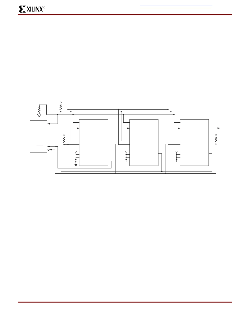
XPLA2 Architecture
Figure 1
shows a high level block diagram of the XCR3320
implementing the XPLA2 architecture. The XPLA2 archi-
tecture is a multi-level, modular hierarchy that consists of
Fast Modules interconnected by a virtual crosspoint switch
called the Global Zero Power Interconnect Array (GZIA).
Each Fast Module accepts 64 bits from the GZIA and out-
puts 64 bits to the GZIA. Each Fast Module is essentially an
80 macrocell CPLD with four logic blocks of 20 macrocells
each inside. There are eight dedicated, low-skew, global
clocks for the device; and each Fast Module has access to
any two of these clocks (there are additional asynchronous
clocks available in the Fast Modules, see
Figure 3
. There
are also Global 3-state (gts) and Global Reset (rstn) pins
that are common to all Fast Modules. When gts is pulled
high, all output buffers in the device will be disabled, caus-
ing all I/O pins to be tri-stated. When rstn is pulled low, all
flip-flops of the device will be reset.
Figure 1: Xilinx XPLA2 CPLD Architecture
reset/OE
SP00665
EEPROM
CE
dout
cclk
din
SLAVE #2
pgrmn
resetn
M2
M1
M0
crcerrn
dout
hdc
cclk
done
M3
V
CC
V
CC
cclk
din
SLAVE #1
pgrmn
resetn
M2
M1
M0
crcerrn
dout
hdc
done
M3
V
CC
cclk
din
MASTER SERIAL
LEAD
pgrmn
resetn
M2
M1
M0
crcerrn
dout
hdc
done
M3
V
CC
V
CC
V
CC
相關(guān)PDF資料 |
PDF描述 |
|---|---|
| XCR3384XL-10FG324C | 384 Macrocell CPLD |
| XCR3384XL-10FG324I | 384 Macrocell CPLD |
| XCR3384XL-10FT256C | 384 Macrocell CPLD |
| XCR3384XL-10FT256I | 384 Macrocell CPLD |
| XCR3384XL-10PQ208C | 384 Macrocell CPLD |
相關(guān)代理商/技術(shù)參數(shù) |
參數(shù)描述 |
|---|---|
| XCR3320-10TQ144C | 制造商:未知廠家 制造商全稱:未知廠家 功能描述: |
| XCR3320-7TQ144C | 制造商:未知廠家 制造商全稱:未知廠家 功能描述: |
| XCR3320-8TQ144I | 制造商:未知廠家 制造商全稱:未知廠家 功能描述: |
| XCR3384XL | 制造商:XILINX 制造商全稱:XILINX 功能描述:384 Macrocell CPLD |
| XCR3384XL_06 | 制造商:XILINX 制造商全稱:XILINX 功能描述:384 Macrocell CPLD |
發(fā)布緊急采購,3分鐘左右您將得到回復(fù)。