- 您現(xiàn)在的位置:買賣IC網(wǎng) > PDF目錄374980 > XC3043L (Xilinx, Inc.) Field Programmable Gate Arrays(現(xiàn)場可編程門陣列) PDF資料下載
參數(shù)資料
| 型號: | XC3043L |
| 廠商: | Xilinx, Inc. |
| 英文描述: | Field Programmable Gate Arrays(現(xiàn)場可編程門陣列) |
| 中文描述: | 現(xiàn)場可編程門陣列(現(xiàn)場可編程門陣列) |
| 文件頁數(shù): | 7/76頁 |
| 文件大?。?/td> | 731K |
| 代理商: | XC3043L |
第1頁第2頁第3頁第4頁第5頁第6頁當(dāng)前第7頁第8頁第9頁第10頁第11頁第12頁第13頁第14頁第15頁第16頁第17頁第18頁第19頁第20頁第21頁第22頁第23頁第24頁第25頁第26頁第27頁第28頁第29頁第30頁第31頁第32頁第33頁第34頁第35頁第36頁第37頁第38頁第39頁第40頁第41頁第42頁第43頁第44頁第45頁第46頁第47頁第48頁第49頁第50頁第51頁第52頁第53頁第54頁第55頁第56頁第57頁第58頁第59頁第60頁第61頁第62頁第63頁第64頁第65頁第66頁第67頁第68頁第69頁第70頁第71頁第72頁第73頁第74頁第75頁第76頁
R
November 9, 1998 (Version 3.1)
7-9
XC3000 Series Field Programmable Gate Arrays
7
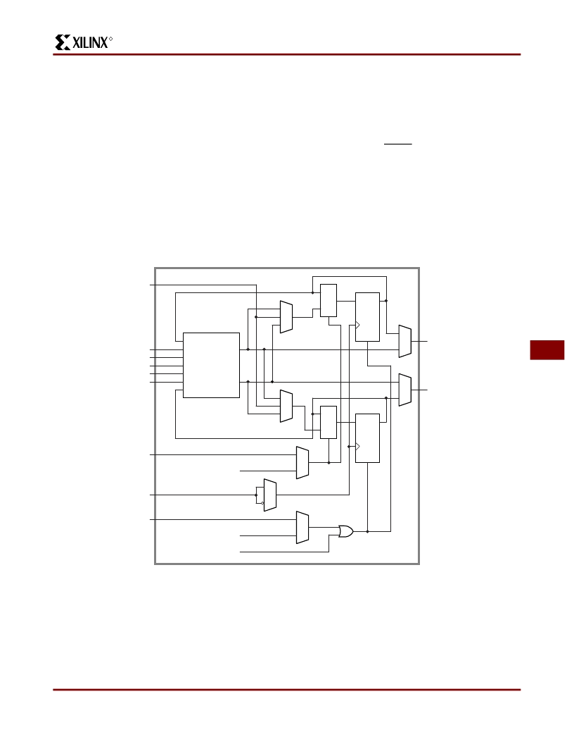
Configurable Logic Block
The array of CLBs provides the functional elements from
which the user’s logic is constructed. The logic blocks are
arranged in a matrix within the perimeter of IOBs. For
example, the XC3020A has 64 such blocks arranged in 8
rows and 8 columns. The development system is used to
compile the configuration data which is to be loaded into
the internal configuration memory to define the operation
and interconnection of each block. User definition of CLBs
and their interconnecting networks may be done by auto-
matic translation from a schematic-capture logic diagram or
optionally by installing library or user macros.
Each CLB has a combinatorial logic section, two flip-flops,
and an internal control section. See
Figure 5
. There are:
five logic inputs (A, B, C, D and E); a common clock input
(K); an asynchronous direct RESET input (RD); and an
enable clock (EC). All may be driven from the interconnect
resources adjacent to the blocks. Each CLB also has two
outputs (X and Y) which may drive interconnect networks.
Data input for either flip-flop within a CLB is supplied from
the function F or G outputs of the combinatorial logic, or the
block input, DI. Both flip-flops in each CLB share the asyn-
chronous RD which, when enabled and High, is dominant
over clocked inputs. All flip-flops are reset by the
active-Low chip input, RESET, or during the configuration
process. The flip-flops share the enable clock (EC) which,
when Low, recirculates the flip-flops’ present states and
inhibits response to the data-in or combinatorial function
inputs on a CLB. The user may enable these control inputs
and select their sources. The user may also select the
clock net input (K), as well as its active sense within each
CLB. This programmable inversion eliminates the need to
route both phases of a clock signal throughout the device.
Q
COMBINATORIAL
FUNCTION
LOGIC
VARIABLES
D
RD
G
F
DIN
G
F
QX
QY
DIN
G
F
G
QY
QX
F
Q
D
RD
ENABLE CLOCK
CLOCK
DIRECT
RESET
1 (ENABLE)
A
B
C
D
E
DI
EC
K
RD
Y
X
X3032
0 (INHIBIT)
(GLOBAL RESET)
CLB OUTPUTS
DATA IN
0
1
0
MUX
1
MUX
Figure 5: Configurable Logic Block.
Each CLB includes a combinatorial logic section, two flip-flops and a program memory controlled multiplexer selection of
function. It has the following:
-
five logic variable inputs A, B, C, D, and E
-
a direct data in DI
-
an enable clock EC
-
a clock (invertible) K
-
an asynchronous direct RESET RD
-
two outputs X and Y
相關(guān)PDF資料 |
PDF描述 |
|---|---|
| XC3030A-6PQ100C | Field Programmable Gate Arrays (XC3000A/L, XC3100A/L) |
| XC3142L-2PC84C | XTAL MTL T/H HC49/US |
| XC3142L-3PC84C | Field Programmable Gate Arrays (XC3000A/L, XC3100A/L) |
| XC3142L-3TQ144C | Field Programmable Gate Arrays (XC3000A/L, XC3100A/L) |
| XC3142L-3VQ160C | Field Programmable Gate Arrays (XC3000A/L, XC3100A/L) |
相關(guān)代理商/技術(shù)參數(shù) |
參數(shù)描述 |
|---|---|
| XC3064 | 制造商:XILINX 制造商全稱:XILINX 功能描述:Logic Cell Array Families |
| XC3064100PC84C | 制造商:XILINX 功能描述:NEW |
| XC3064-100PC84C | 制造商:Xilinx 功能描述: 制造商:Xilinx 功能描述:Field-Programmable Gate Array, 224 Cell, 84 Pin, Plastic, PLCC |
| XC3064-100PC84I | 制造商:未知廠家 制造商全稱:未知廠家 功能描述:Field Programmable Gate Array (FPGA) |
| XC3064-100PG132M | 制造商:Xilinx 功能描述: |
發(fā)布緊急采購,3分鐘左右您將得到回復(fù)。