- 您現(xiàn)在的位置:買(mǎi)賣(mài)IC網(wǎng) > PDF目錄231491 > WEDPN16M72VR-100B2C (WHITE ELECTRONIC DESIGNS CORP) 16M X 72 SYNCHRONOUS DRAM MODULE, 6 ns, PBGA219 PDF資料下載
參數(shù)資料
| 型號(hào): | WEDPN16M72VR-100B2C |
| 廠商: | WHITE ELECTRONIC DESIGNS CORP |
| 元件分類(lèi): | DRAM |
| 英文描述: | 16M X 72 SYNCHRONOUS DRAM MODULE, 6 ns, PBGA219 |
| 封裝: | 25 X 25 MM, PLASTIC, BGA-219 |
| 文件頁(yè)數(shù): | 11/13頁(yè) |
| 文件大?。?/td> | 470K |
| 代理商: | WEDPN16M72VR-100B2C |
第1頁(yè)第2頁(yè)第3頁(yè)第4頁(yè)第5頁(yè)第6頁(yè)第7頁(yè)第8頁(yè)第9頁(yè)第10頁(yè)當(dāng)前第11頁(yè)第12頁(yè)第13頁(yè)
7
White Electronic Designs Corporation (602) 437-1520 www.whiteedc.com
White Electronic Designs
WEDPN16M72VR-XB2X
January 2005
Rev. 1
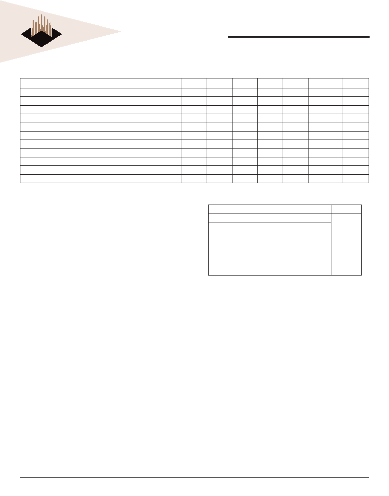
REGISTER FUNCTION TABLE
INPUTS
OUTPUT
OE
LE
CLK
A
Y
HX
X
Z
LL
X
L
LL
X
H
LH
I
L
LH
I
H
LH
L or H
X
Y0(1)
NOTE: 1. Output level before the indicated steady-state input conditions were
established.
COMMAND INHIBIT
The COMMAND INHIBIT function prevents new commands
from being executed by the SDRAM, regardless of whether
the CLK signal is enabled. The SDRAM is effectively
deselected. Operations already in progress are not
affected.
NO OPERATION (NOP)
The NO OPERATION (NOP) command is used to perform
a NOP to an SDRAM which is selected (CS# is LOW).
This prevents unwanted commands from being registered
during idle or wait states. Operations already in progress
are not affected.
LOAD MODE REGISTER
The Mode Register is loaded via inputs A0-11. See Mode
Register heading in the Register Denition section. The
LOAD MODE REGISTER command can only be issued
when all banks are idle, and a subsequent executable
command cannot be issued until tMRD is met.
ACTIVE
The ACTIVE command is used to open (or activate) a row in
a particular bank for a subsequent access. The value on the
BA0, BA1 inputs selects the bank, and the address provided
on inputs A0-11 selects the row. This row remains active
(or open) for accesses until a PRECHARGE command is
issued to that bank. A PRECHARGE command must be
issued before opening a different row in the same bank.
READ
The READ command is used to initiate a burst read
access to an active row. The value on the BA0, BA1 inputs
selects the bank, and the address provided on inputs A0-8
selects the starting column location. The value on input
A10 determines whether or not AUTO PRECHARGE is
used. If AUTO PRECHARGE is selected, the row being
accessed will be precharged at the end of the READ
burst; if AUTO PRECHARGE is not selected, the row will
remain open for subsequent accesses. Read data appears
on the I/Os subject to the logic level on the DQM inputs
TRUTH TABLE — COMMANDS AND DQM OPERATION (NOTE 1)
NAME (FUNCTION)
CS#
RAS#
CAS#
WE#
DQM
ADDR
I/Os
COMMAND INHIBIT (NOP)
H
X
NO OPERATION (NOP)
L
H
X
ACTIVE (Select bank and activate row) ( 3)
L
H
X
Bank/Row
X
READ (Select bank and column, and start READ burst) (4)
L
H
L
H
L/H 8
Bank/Col
X
WRITE (Select bank and column, and start WRITE burst) (4)
L
H
L
L/H 8
Bank/Col
Valid
BURST TERMINATE
L
H
L
X
Active
PRECHARGE (Deactivate row in bank or banks) ( 5)
L
H
L
X
Code
X
AUTO REFRESH or SELF REFRESH (Enter self refresh mode) (6, 7)
L
H
X
LOAD MODE REGISTER (2)
L
X
Op-Code
X
Write Enable/Output Enable (8)
–
L
–
Active
Write Inhibit/Output High-Z (8)
–
H
–
High-Z
NOTES:
1. CKE is HIGH for all commands shown except SELF REFRESH.
2. A0-11 dene the op-code written to the Mode Register and A12 should be driven low.
3. A0-12 provide row address, and BA0, BA1 determine which bank is made active.
4. A0-8 provide column address; A10 HIGH enables the auto precharge feature
(nonpersistent), while A10 LOW disables the auto precharge feature; BA0, BA1
determine which bank is being read from or written to.
5. A10 LOW: BA0, BA1 determine the bank being precharged. A10 HIGH: All banks
precharged and BA0, BA1 are “Don’t Care.”
6. This command is AUTO REFRESH if CKE is HIGH; SELF REFRESH if CKE is LOW.
7. Internal refresh counter controls row addressing; all inputs and I/Os are “Don’t Care”
except for CKE.
8. Activates or deactivates the I/Os during WRITEs (zero-clock delay) and READs (two-
clock delay).
相關(guān)PDF資料 |
PDF描述 |
|---|---|
| WEDPN16M64VR-100B2C | 16M X 64 SYNCHRONOUS DRAM MODULE, 6 ns, PBGA219 |
| W3DG63126V10D2 | 128M X 64 SYNCHRONOUS DRAM MODULE, 6 ns, DMA168 |
| W3E232M16S-266STIG | 64M X 16 DDR DRAM, 0.7 ns, PDSO66 |
| WPS256K16T-20LJC | 256K X 16 STANDARD SRAM, 20 ns, PDSO44 |
| WMF256K8-70FEM5A | 256K X 8 FLASH 5V PROM, 70 ns, CDFP32 |
相關(guān)代理商/技術(shù)參數(shù) |
參數(shù)描述 |
|---|---|
| WEDPN16M72VR-100B2I | 制造商:White Electronic Designs 功能描述:WEDPN16M72VR-100B2I - Bulk |
| WEDPN16M72VR-100B2M | 制造商:WEDC 制造商全稱:White Electronic Designs Corporation 功能描述:16MX72 REGISTERED SYNCHRONOUS DRAM |
| WEDPN16M72VR-100BC | 制造商:Microsemi Corporation 功能描述:16M X 72 SDRAM MODULE W/REGISTERED BUFFERS, 3.3V, 100 MHZ, 2 - Bulk 制造商:White Electronic Designs 功能描述:16M X 72 SDRAM MODULE W/REGISTERED BUFFERS, 3.3V, 100 MHZ, 2 - Bulk |
| WEDPN16M72VR-100BI | 制造商:Microsemi Corporation 功能描述:16M X 72 SDRAM MODULE W/REGISTERED BUFFERS, 3.3V, 100 MHZ, 2 - Bulk 制造商:White Electronic Designs 功能描述:16M X 72 SDRAM MODULE W/REGISTERED BUFFERS, 3.3V, 100 MHZ, 2 - Bulk |
| WEDPN16M72VR-100BM | 制造商:Microsemi Corporation 功能描述:16M X 72 SDRAM MODULE W/REGISTERED BUFFERS, 3.3V, 100 MHZ, 2 - Bulk 制造商:White Electronic Designs 功能描述:16M X 72 SDRAM MODULE W/REGISTERED BUFFERS, 3.3V, 100 MHZ, 2 - Bulk |
發(fā)布緊急采購(gòu),3分鐘左右您將得到回復(fù)。