- 您現(xiàn)在的位置:買賣IC網(wǎng) > PDF目錄231491 > WEDPN16M72VR-100B2C (WHITE ELECTRONIC DESIGNS CORP) 16M X 72 SYNCHRONOUS DRAM MODULE, 6 ns, PBGA219 PDF資料下載
參數(shù)資料
| 型號: | WEDPN16M72VR-100B2C |
| 廠商: | WHITE ELECTRONIC DESIGNS CORP |
| 元件分類: | DRAM |
| 英文描述: | 16M X 72 SYNCHRONOUS DRAM MODULE, 6 ns, PBGA219 |
| 封裝: | 25 X 25 MM, PLASTIC, BGA-219 |
| 文件頁數(shù): | 10/13頁 |
| 文件大小: | 470K |
| 代理商: | WEDPN16M72VR-100B2C |
6
White Electronic Designs Corporation (602) 437-1520 www.whiteedc.com
White Electronic Designs
WEDPN16M72VR-XB2X
January 2005
Rev. 1
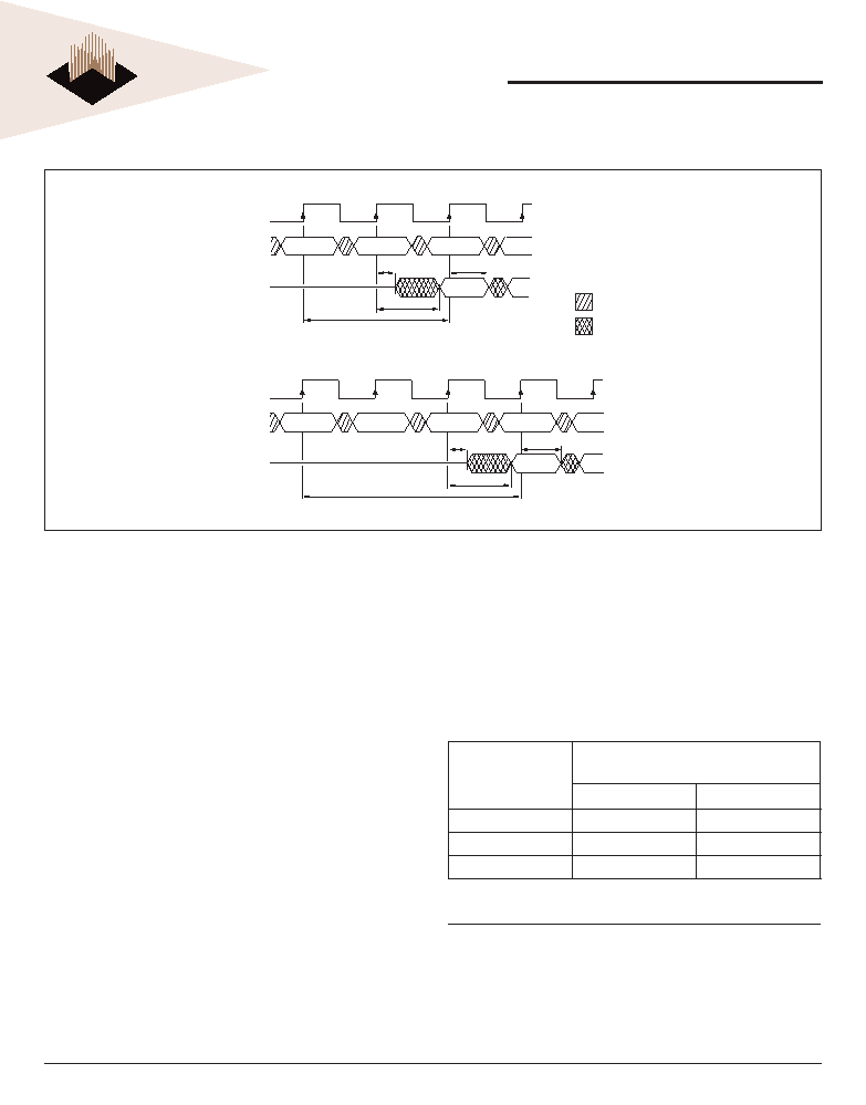
CAS LATENCY
The CAS latency is the delay, in clock cycles, between
the registration of a READ command and the availability
of the rst piece of output data. The latency can be set to
two or three clocks.
If a READ command is registered at clock edge n, and
the latency is m clocks, the data will be available by clock
edge n+m. The I/Os will start driving as a result of the clock
edge one cycle earlier (n + m - 1), and provided that the
relevant access times are met, the data will be valid by
clock edge n + m. For example, assuming that the clock
cycle time is such that all relevant access times are met,
if a READ command is registered at T0 and the latency
is programmed to two clocks, the I/Os will start driving
after T1 and the data will be valid by T2. Table 2 below
indicates the operating frequencies at which each CAS
latency setting can be used.
Reserved states should not be used as unknown operation
or incompatibility with future versions may result.
OPERATING MODE
The normal operating mode is selected by setting M7and
M8 to zero; the other combinations of values for M7 and
M8 are reserved for future use and/or test modes. The
programmed burst length applies to both READ and
WRITE bursts.
Test modes and reserved states should not be used
because unknown operation or incompatibility with future
versions may result.
WRITE BURST MODE
When M9 = 0, the burst length programmed via M0-M2
applies to both READ and WRITE bursts; when M9 = 1,
the programmed burst length applies to READ bursts, but
write accesses are single-location (nonburst) accesses.
TABLE 2 - CAS LATENCY
SPEED
ALLOWABLE OPERATING
FREQUENCY (MHz)
CAS LATENCY = 2
CAS LATENCY = 3
-100
≤66
≤100
-125
≤100
≤125
-133
≤100
≤133
COMMANDS
The Truth Table provides a quick reference of available
commands. This is followed by a written description of each
command. Three additional Truth Tables appear following
the Operation section; these tables provide current state/
next state information.
FIGURE 4 – CAS LATENCY
CLK
Command
I/O
CLK
Command
I/O
T0
T1
T2
T3
T0
T1
T2
T3
T4
READ
NOP
CAS Latency = 2
DOUT
tLZ
tOH
tAC
READ
NOP
DOUT
tLZ
tOH
tAC
CAS Latency = 3
DON'T CARE
UNDEFINED
相關(guān)PDF資料 |
PDF描述 |
|---|---|
| WEDPN16M64VR-100B2C | 16M X 64 SYNCHRONOUS DRAM MODULE, 6 ns, PBGA219 |
| W3DG63126V10D2 | 128M X 64 SYNCHRONOUS DRAM MODULE, 6 ns, DMA168 |
| W3E232M16S-266STIG | 64M X 16 DDR DRAM, 0.7 ns, PDSO66 |
| WPS256K16T-20LJC | 256K X 16 STANDARD SRAM, 20 ns, PDSO44 |
| WMF256K8-70FEM5A | 256K X 8 FLASH 5V PROM, 70 ns, CDFP32 |
相關(guān)代理商/技術(shù)參數(shù) |
參數(shù)描述 |
|---|---|
| WEDPN16M72VR-100B2I | 制造商:White Electronic Designs 功能描述:WEDPN16M72VR-100B2I - Bulk |
| WEDPN16M72VR-100B2M | 制造商:WEDC 制造商全稱:White Electronic Designs Corporation 功能描述:16MX72 REGISTERED SYNCHRONOUS DRAM |
| WEDPN16M72VR-100BC | 制造商:Microsemi Corporation 功能描述:16M X 72 SDRAM MODULE W/REGISTERED BUFFERS, 3.3V, 100 MHZ, 2 - Bulk 制造商:White Electronic Designs 功能描述:16M X 72 SDRAM MODULE W/REGISTERED BUFFERS, 3.3V, 100 MHZ, 2 - Bulk |
| WEDPN16M72VR-100BI | 制造商:Microsemi Corporation 功能描述:16M X 72 SDRAM MODULE W/REGISTERED BUFFERS, 3.3V, 100 MHZ, 2 - Bulk 制造商:White Electronic Designs 功能描述:16M X 72 SDRAM MODULE W/REGISTERED BUFFERS, 3.3V, 100 MHZ, 2 - Bulk |
| WEDPN16M72VR-100BM | 制造商:Microsemi Corporation 功能描述:16M X 72 SDRAM MODULE W/REGISTERED BUFFERS, 3.3V, 100 MHZ, 2 - Bulk 制造商:White Electronic Designs 功能描述:16M X 72 SDRAM MODULE W/REGISTERED BUFFERS, 3.3V, 100 MHZ, 2 - Bulk |
發(fā)布緊急采購,3分鐘左右您將得到回復(fù)。