- 您現(xiàn)在的位置:買賣IC網 > PDF目錄359439 > VT83C469 (Electronic Theatre Controls, Inc.) PCMCIA Socket Controller PDF資料下載
參數資料
| 型號: | VT83C469 |
| 廠商: | Electronic Theatre Controls, Inc. |
| 英文描述: | PCMCIA Socket Controller |
| 中文描述: | PCMCIA插槽控制器 |
| 文件頁數: | 23/36頁 |
| 文件大?。?/td> | 156K |
| 代理商: | VT83C469 |
第1頁第2頁第3頁第4頁第5頁第6頁第7頁第8頁第9頁第10頁第11頁第12頁第13頁第14頁第15頁第16頁第17頁第18頁第19頁第20頁第21頁第22頁當前第23頁第24頁第25頁第26頁第27頁第28頁第29頁第30頁第31頁第32頁第33頁第34頁第35頁第36頁
VIA Technologies, Inc.
Preliminary
VT83C469
23
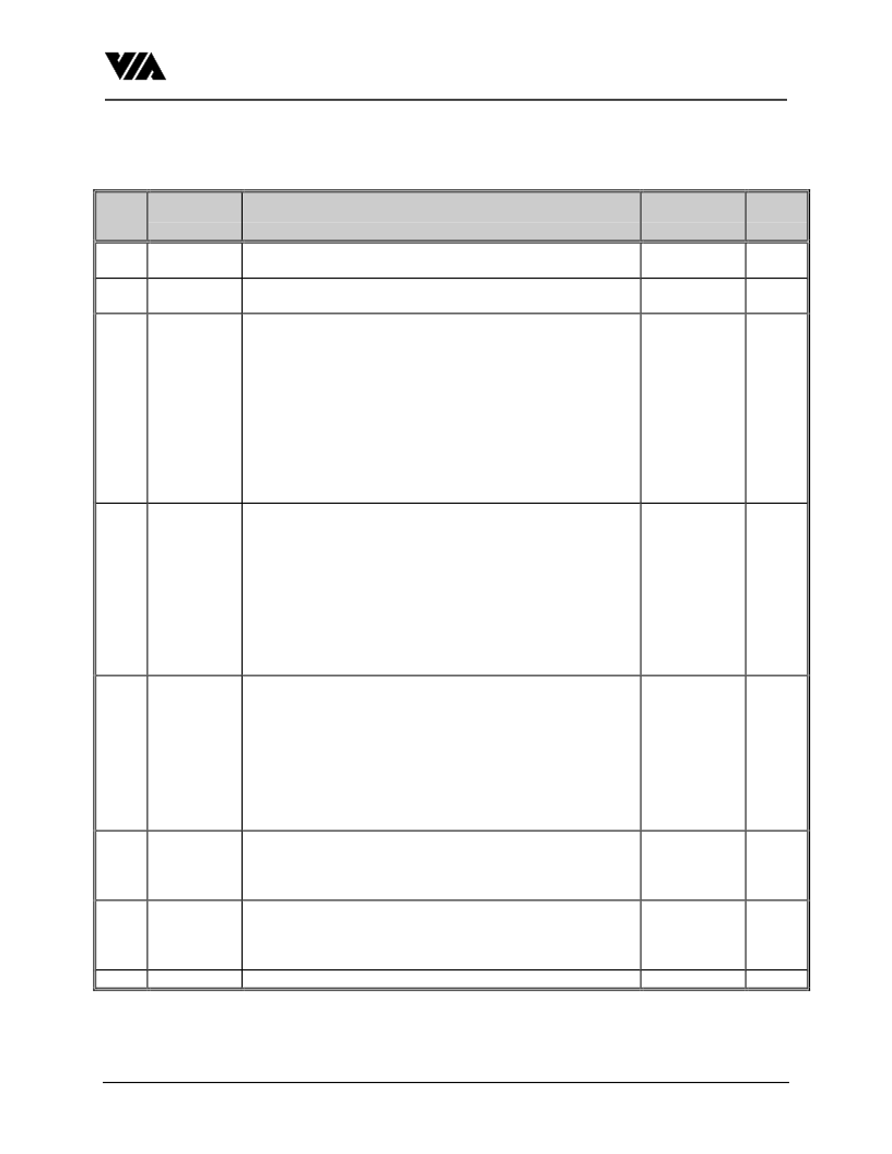
VT83C469 P
IN
D
ESCRIPTION
B
US
T
YPE
I
S
IGNAL
D
ESCRIPTION
P
IN
T
YPE
AEN
System Address Enable. High during DMA cycles, low
otherwise
Bus Address Latch Enable. An active high input used to latch
LA [23:17] at the beginning of the bus cycle
If BVD1 is negated by a memory PC Card with a battery, it
indicates that the battery is no longer serviceable and data is lost.
204
I
I
BALE
205
I
S
BVD1
(STSCHG#/
RI#)
For I/O PC Cards, this signal is held high when either or both the
Signal on Change bit and Changed bit in the Card Status Register
on the PC Card are set to zero. When both of the bits are one, the
signal is held low. The Changed bit is the logical OR of the bits
CVBAT1, CVBAT2, CWP and CBSYRDY in the Pin
Replacement Register on the PC Card. Or this pin is connected
to Ring Indicate, which is qualified by Ring Indicate Enable to be
passed on to the *RIO pin.
BVD1 and BVD2 are generated by memory PC Cards with
onboard batteries. These signals indicate the health of the
battery. Both are asserted high when the battery is in good
condition. When BVD2 is negated while BVD1 is still asserted,
the battery should be replaced, although data integrity on the
memory PC Card is still assured.
54, 125
I
S
BVD2
(SPKR#)
When the I/O interface is selected, BVD2 may be used to provide
a single amplitude Digital Audio waveform intended to be passed
through to the system's speaker without signal conditioning.
Card Address
52, 123
I
S
CA [25:0]
15,19, 21, 23-
26, 28, 31, 33-
41, 43-44, 46,
48, 50-51, 53,
86, 90, 92, 94-
99, 102, 104-
107, 109-115,
117, 119, 121-
122, 124
63, 3, 134, 74
O
S
CD# [2:1]
Detects proper card insertion. The signals are connected to
ground internally on the PC Card and will be forced low
whenever a card is placed in a host socket. Status is available to
software through the Interface Status Register.
Active low card enable signals. CE#1 is used to enable even
bytes, CE#2 for odd bytes. A multiplexing scheme based on A0,
CE#1, CE#2 allows 8-bit hosts to access all data on Card Data
[7:0] if desired.
System Clock
I
S
CE# [2:1]
89, 83, 18, 11
O
I
CLK
187
I
相關PDF資料 |
PDF描述 |
|---|---|
| VT83C572 | PCI TO USB CONTROLLER |
| VT83N1 | |
| VT80N1 | |
| VT80N2 | |
| VT83N2 | |
相關代理商/技術參數 |
參數描述 |
|---|---|
| VT83C572 | 制造商:未知廠家 制造商全稱:未知廠家 功能描述:PCI TO USB CONTROLLER |
| VT83CT | 制造商:PERKINELMER 制造商全稱:PerkinElmer Optoelectronics 功能描述:Photoconductive Cells and Analog Optoisolators (Vactrols) |
| VT83D223 | 制造商:未知廠家 制造商全稱:未知廠家 功能描述: |
| VT83D263/2 | 制造商:未知廠家 制造商全稱:未知廠家 功能描述: |
| VT83E303 | 制造商:未知廠家 制造商全稱:未知廠家 功能描述: |
發(fā)布緊急采購,3分鐘左右您將得到回復。