- 您現(xiàn)在的位置:買賣IC網(wǎng) > PDF目錄359432 > VSC9142 (VITESSE SEMICONDUCTOR CORP) SONET/SDH 2.5Gbps Transport Terminating Transceiver PDF資料下載
參數(shù)資料
| 型號: | VSC9142 |
| 廠商: | VITESSE SEMICONDUCTOR CORP |
| 元件分類: | 數(shù)字傳輸電路 |
| 英文描述: | SONET/SDH 2.5Gbps Transport Terminating Transceiver |
| 中文描述: | MUX/DEMUX, PBGA320 |
| 封裝: | TBGA-320 |
| 文件頁數(shù): | 20/30頁 |
| 文件大小: | 259K |
| 代理商: | VSC9142 |
第1頁第2頁第3頁第4頁第5頁第6頁第7頁第8頁第9頁第10頁第11頁第12頁第13頁第14頁第15頁第16頁第17頁第18頁第19頁當(dāng)前第20頁第21頁第22頁第23頁第24頁第25頁第26頁第27頁第28頁第29頁第30頁
G56054, Rev 1.0
VSC9142
STS-48c Physical Layer Packet/ATMOver SONET/SDH Device
Page 20
1.0 Product Description
.
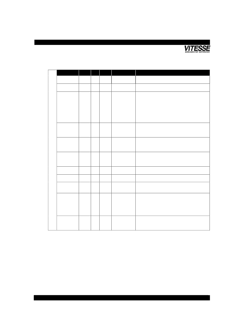
Table 1.1
Hardware Signal Definitions (2 of 12)
Pin Label
TLOUTSER-
TLOUTSER+
TLCLKSER-
TLCLKSER+
TLOUT4[0]-
TLOUT4[0]+
TLOUT4[1]-
TLOUT4[1]+
TLOUT4[2]-
TLOUT4[2]+
TLOUT4[3]-
TLOUT4[3]+
TLPRTY4-
TLPRTY4+
Pad
N24
M24
R24
P24
V23
V22
V24
W23
Y22
W21
AA24
AA23
U23
U22
I/O
O
Type
PECL
Signal Name
Serial Line
Transmt Data
Serial Line
Transmt Clock
Parallel Line
Transmt Data
Description
Serial line data output.
O
PECL
Serial line clock output
O
LVDS
This is the parallel line-side transmt data bus for the outgoing
STS-48c/STM-16 AU-4-16c data stream TLOUT4[3] is the
most significant and first transmtted bit in the serial data
stream TLOUT4[3..0] is latched out the rising edge of
TLCLK4+, but is centered about TLCLK4O-. TLOUT[3..0]+ are
the true signal values.
O
LVDS
Parallel Line
Transmt Parity
This is a programmable (even/odd) parity bit for parallel line
transmt data TLOUT4[3..0]. TLPRTY4 is latched out on the
rising edge of TLCLK4+, but is centered about TLCLK4O-.
TLPRTY4+ is the true signal value.
This is the reference clock input for the parallel line-transmt
data carried in TLOUT4[3..0]+/-. The nomnal frequency is
622.08 MHz for STS-48c/STM-16 AU-4-16c operation.
TLCLK4+ is the true signal value.
This output is the looped version of the reference clock input
TLCLK4+/-. The nomnal frequency is 622.08 MHz for STS-
48c/STM-16 AU-4-16c operation. TLCLK4O+ is the true signal
value.
This input is the reference clock used for the clock multiplier
unit.
This output indicates the presense of clock transistions on
CMUREFCLK+/-. The signal is active high.
This output indicatest the lock status of the PLL within the
CMU with respect to CMUREFCLK+/-. The signal is active
high.
These inputs select which frequency is to be expected on
CMUREFCLK+/-. The binary combination of the two pins are
described below (CMUREFSEL0 noted first).
00 78 MHz
01 155 MHz
10 311 MHz
These inputs are brought off-chip to connect to a capacitor
which completes the CMU loop filter. CMUFILTER+ should be
connected to one side of a 0.1uF capacitor while CMUFILTER-
should be connected to the other side of the capacitor.
TLCLK4-
TLCLK4+
T24
U24
I
LVDS
Parallel Line
Transmt Clock
TLCLK4O-
TLCLK4O+
Y24
W24
O
LVDS
Parallel Line
Transmt Clock
Out
CMUREFCLK-
CMUREFCLK+
CMUREFDET
N23
M23
AC17
I
PECL
CMU Reference
Clock
CMU Reference
Clock Detect
CMU Lock Detect
O
TTL
CMULOCKDET
AC16
O
TTL
CMUREFSEL1
CMUREFSEL0
AB16
AA16
I
TTL
CMU Reference
Clock Select
P
CMUFILTER-
CMUFILTER+
L22
L21
I
N/A
CMU Loop Filter
相關(guān)PDF資料 |
PDF描述 |
|---|---|
| VSC9180 | VSC9180 Arapahoe - 2.5G SONET/SDH Backplane Transceiver |
| VSC9182 | VSC9182 - 40G STS-1 Time Slot Interchange |
| VSC9186 | VSC9186 Killington - Quad STS-48/STM-16 and STS-192/STM-64 Line Interface |
| VSC9187 | VSC9187 Bromley - 3045 x 3045 VT1.5 TSI Switch Fabric |
| VSC9191 | 100 Gbps (40 x 40) SONET/SDH TSI Switch with Dual Rate I/O |
相關(guān)代理商/技術(shù)參數(shù) |
參數(shù)描述 |
|---|---|
| VSC9180 | 制造商:VITESSE 制造商全稱:Vitesse Semiconductor Corporation 功能描述:VSC9180 Arapahoe - 2.5G SONET/SDH Backplane Transceiver |
| VSC9182 | 制造商:VITESSE 制造商全稱:Vitesse Semiconductor Corporation 功能描述:VSC9182 - 40G STS-1 Time Slot Interchange |
| VSC9186 | 制造商:VITESSE 制造商全稱:Vitesse Semiconductor Corporation 功能描述:VSC9186 Killington - Quad STS-48/STM-16 and STS-192/STM-64 Line Interface |
| VSC9186ZB/D | 制造商:Vitesse Semiconductor Corporation 功能描述:CHIPSET |
| VSC9187 | 制造商:VITESSE 制造商全稱:Vitesse Semiconductor Corporation 功能描述:VSC9187 Bromley - 3045 x 3045 VT1.5 TSI Switch Fabric |
發(fā)布緊急采購,3分鐘左右您將得到回復(fù)。