- 您現(xiàn)在的位置:買賣IC網(wǎng) > PDF目錄359431 > VSC8116QP1 (VITESSE SEMICONDUCTOR CORP) ATM/SONET/SDH 622/155Mb/s Transceiver Mux/Demux with Integrated Clock Generation PDF資料下載
參數(shù)資料
| 型號(hào): | VSC8116QP1 |
| 廠商: | VITESSE SEMICONDUCTOR CORP |
| 元件分類: | 數(shù)字傳輸電路 |
| 英文描述: | ATM/SONET/SDH 622/155Mb/s Transceiver Mux/Demux with Integrated Clock Generation |
| 中文描述: | TRANSCEIVER, PQFP64 |
| 封裝: | 10 X 10 MM, HEAT SPREADER, PLASTIC, QFP-64 |
| 文件頁(yè)數(shù): | 3/20頁(yè) |
| 文件大?。?/td> | 358K |
| 代理商: | VSC8116QP1 |
第1頁(yè)第2頁(yè)當(dāng)前第3頁(yè)第4頁(yè)第5頁(yè)第6頁(yè)第7頁(yè)第8頁(yè)第9頁(yè)第10頁(yè)第11頁(yè)第12頁(yè)第13頁(yè)第14頁(yè)第15頁(yè)第16頁(yè)第17頁(yè)第18頁(yè)第19頁(yè)第20頁(yè)
G52220-0, Rev 4.1
1/8/00
VITESSE
SEMICONDUCTOR CORPORATION
741 Calle Plano, Camarillo, CA 93012 805/388-3700 FAX: 805/987-5896
Page 3
VITESSE
Data Sheet
VSC8116
ATM/SONET/SDH 622/155Mb/s Transceiver
Mux/Demux with Integrated Clock Generation
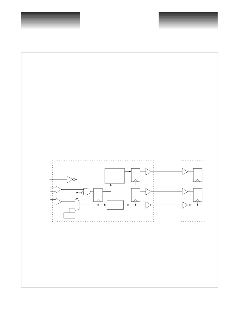
Receive Section
High speed Non-Return to Zero (NRZ) serial data at 155Mb/s or 622Mb/s are received by the RXDATAIN
inputs. The corresponding clock is received by the RXCLKIN inputs. RXDATAIN is clocked in on the rising
edge of RXCLKIN+. See Figure 2. The serial data is converted to byte-wide parallel data and presented on
RXOUT[7:0] pins. A divide-by-8 version of the high-speed clock (RXLSCKOUT) should be used to synchro-
nize the byte-serial RXOUT[7:0] data with the receive portion of the UNI device.
The receive section also includes frame detection and recovery circuitry which detects the SONET/SDH
frame, aligns the received serial data on byte boundaries, and initiates a frame pulse on FP coincident with the
byte aligned data. The frame recovery is initiated when OOF is held high which must occur at least 4 byte clock
cycles before the A1A2 boundary. The OOF input control is a level-sensitive signal, and the VSC8116 will con-
tinually perform frame detection and recovery as long as this pin is held high even if 1 or more frames has been
detected. Frame detection and recovery occurs when a series of three A1 bytes followed by three A2 bytes has
been detected. The parallel output data on RXOUT[7:0] will be byte aligned starting on the third A2 byte. When
a frame is detected, a single byte clock period long pulse is generated on FP which is synchronized with the
byte-aligned third A2 byte on RXOUT[7:0]. The frame detector sends an FP pulse only if OOF is high or if a
frame was detected while OOF was being pulled low.
Figure 2: Data and Clock Receive Block Diagram
Loss of Signal
During a LOS condition, the VSC8116 forces the receive data low which is an indication for any downstream
equipment that an optical interface failure has occurred. The receive section is clocked by the transmit section’s
D Q
D Q
D Q
0
1
Divide-by-8
CMU
D Q
PM5355
D Q
RXOUT[7:0]
FP
RXLSCKOUT
VSC8116
RXDATAIN+
RXDATAIN-
RXCLKIN+
RXCLKIN-
LOSTTL
1:8 Serial
to Parallel
相關(guān)PDF資料 |
PDF描述 |
|---|---|
| VSC8116QP2 | ATM/SONET/SDH 622/155Mb/s Transceiver Mux/Demux with Integrated Clock Generation |
| VSC8117 | ATM/SONET/SDH 622/155 Mb/s Transceiver Mux/Demux with Integrated Clock Generation and Clock Recovery |
| VSC8117QP | GIGATRUE 550 CAT PATCH CBL SNAGLSS 20FT BL 25 PK |
| VSC8117QP1 | GIGATRUE 550 CAT6 PATCH 25 FT, SNAGLESS, BLUE |
| VSC8117QP2 | GIGATRUE 550 CAT6 PATCH 30 FT. SNAGLESS BLUE |
相關(guān)代理商/技術(shù)參數(shù) |
參數(shù)描述 |
|---|---|
| VSC8116QP2 | 制造商:VITESSE 制造商全稱:Vitesse Semiconductor Corporation 功能描述:ATM/SONET/SDH 622/155Mb/s Transceiver Mux/Demux with Integrated Clock Generation |
| VSC8117 | 制造商:VITESSE 制造商全稱:Vitesse Semiconductor Corporation 功能描述:ATM/SONET/SDH 622/155 Mb/s Transceiver Mux/Demux with Integrated Clock Generation and Clock Recovery |
| VSC8117QP | 制造商:Vitesse Semiconductor Corporation 功能描述:Telecomm/Datacomm, Other |
| VSC8117QP1 | 制造商:VITESSE 制造商全稱:Vitesse Semiconductor Corporation 功能描述:ATM/SONET/SDH 622/155 Mb/s Transceiver Mux/Demux with Integrated Clock Generation and Clock Recovery |
| VSC8117QP2 | 制造商:VITESSE 制造商全稱:Vitesse Semiconductor Corporation 功能描述:ATM/SONET/SDH 622/155 Mb/s Transceiver Mux/Demux with Integrated Clock Generation and Clock Recovery |
發(fā)布緊急采購(gòu),3分鐘左右您將得到回復(fù)。