- 您現(xiàn)在的位置:買賣IC網(wǎng) > PDF目錄297644 > UPD70F3261YGF-JBT-A 32-BIT, FLASH, 32 MHz, MICROCONTROLLER, PQFP100 PDF資料下載
參數(shù)資料
| 型號(hào): | UPD70F3261YGF-JBT-A |
| 元件分類: | 微控制器/微處理器 |
| 英文描述: | 32-BIT, FLASH, 32 MHz, MICROCONTROLLER, PQFP100 |
| 封裝: | 14 X 20 MM, PLASTIC, QFP-100 |
| 文件頁(yè)數(shù): | 91/129頁(yè) |
| 文件大小: | 8549K |
| 代理商: | UPD70F3261YGF-JBT-A |
第1頁(yè)第2頁(yè)第3頁(yè)第4頁(yè)第5頁(yè)第6頁(yè)第7頁(yè)第8頁(yè)第9頁(yè)第10頁(yè)第11頁(yè)第12頁(yè)第13頁(yè)第14頁(yè)第15頁(yè)第16頁(yè)第17頁(yè)第18頁(yè)第19頁(yè)第20頁(yè)第21頁(yè)第22頁(yè)第23頁(yè)第24頁(yè)第25頁(yè)第26頁(yè)第27頁(yè)第28頁(yè)第29頁(yè)第30頁(yè)第31頁(yè)第32頁(yè)第33頁(yè)第34頁(yè)第35頁(yè)第36頁(yè)第37頁(yè)第38頁(yè)第39頁(yè)第40頁(yè)第41頁(yè)第42頁(yè)第43頁(yè)第44頁(yè)第45頁(yè)第46頁(yè)第47頁(yè)第48頁(yè)第49頁(yè)第50頁(yè)第51頁(yè)第52頁(yè)第53頁(yè)第54頁(yè)第55頁(yè)第56頁(yè)第57頁(yè)第58頁(yè)第59頁(yè)第60頁(yè)第61頁(yè)第62頁(yè)第63頁(yè)第64頁(yè)第65頁(yè)第66頁(yè)第67頁(yè)第68頁(yè)第69頁(yè)第70頁(yè)第71頁(yè)第72頁(yè)第73頁(yè)第74頁(yè)第75頁(yè)第76頁(yè)第77頁(yè)第78頁(yè)第79頁(yè)第80頁(yè)第81頁(yè)第82頁(yè)第83頁(yè)第84頁(yè)第85頁(yè)第86頁(yè)第87頁(yè)第88頁(yè)第89頁(yè)第90頁(yè)當(dāng)前第91頁(yè)第92頁(yè)第93頁(yè)第94頁(yè)第95頁(yè)第96頁(yè)第97頁(yè)第98頁(yè)第99頁(yè)第100頁(yè)第101頁(yè)第102頁(yè)第103頁(yè)第104頁(yè)第105頁(yè)第106頁(yè)第107頁(yè)第108頁(yè)第109頁(yè)第110頁(yè)第111頁(yè)第112頁(yè)第113頁(yè)第114頁(yè)第115頁(yè)第116頁(yè)第117頁(yè)第118頁(yè)第119頁(yè)第120頁(yè)第121頁(yè)第122頁(yè)第123頁(yè)第124頁(yè)第125頁(yè)第126頁(yè)第127頁(yè)第128頁(yè)第129頁(yè)
CHAPTER 3 CPU FUNCTION
User’s Manual U16541EJ5V1UD
64
3.3
Operation Modes
The V850ES/SG2 and V850ES/SG2-H have the following operation modes.
(1) Normal operation mode
In this mode, each pin related to the bus interface is set to the port mode after system reset has been released.
Execution branches to the reset entry address of the internal ROM, and then instruction processing is started.
(2) Flash memory programming mode
In this mode, the internal flash memory can be programmed by using a flash memory programmer.
The following products are on-chip flash memory versions of the V850ES/SG2 and V850ES/SG2-H.
μPD70F3261, 70F3261Y, 70F3263, 70F3263Y, 70F3271, 70F3271Y, 70F3273, 70F3273Y, 70F3281,
70F3281Y, 70F3283, 70F3283Y, 70F3263HY, 70F3273HY, 70F3283HY
(3) On-chip debug mode
The V850ES/SG2 and V850ES/SG2-H are provided with an on-chip debug function that employs the JTAG
(Joint Test Action Group) communication specifications and that is executed via an on-chip debug emulator.
The on-chip debug function is provided only in the flash memory versions.
For details, see CHAPTER 31 ON-CHIP DEBUG FUNCTION.
3.3.1
Specifying operation mode
Specify the operation mode by using the FLMD0 and FLMD1 pins.
In the normal mode, input a low level to the FLMD0/IC pin after the reset status has been released and before the
oscillation stabilization time expires and the firmware operation is completed.
In the flash memory programming mode, a high level is input to the FLMD0 pin from the flash memory programmer
if a flash memory programmer is connected, but it must be input from an external circuit in the self-programming
mode.
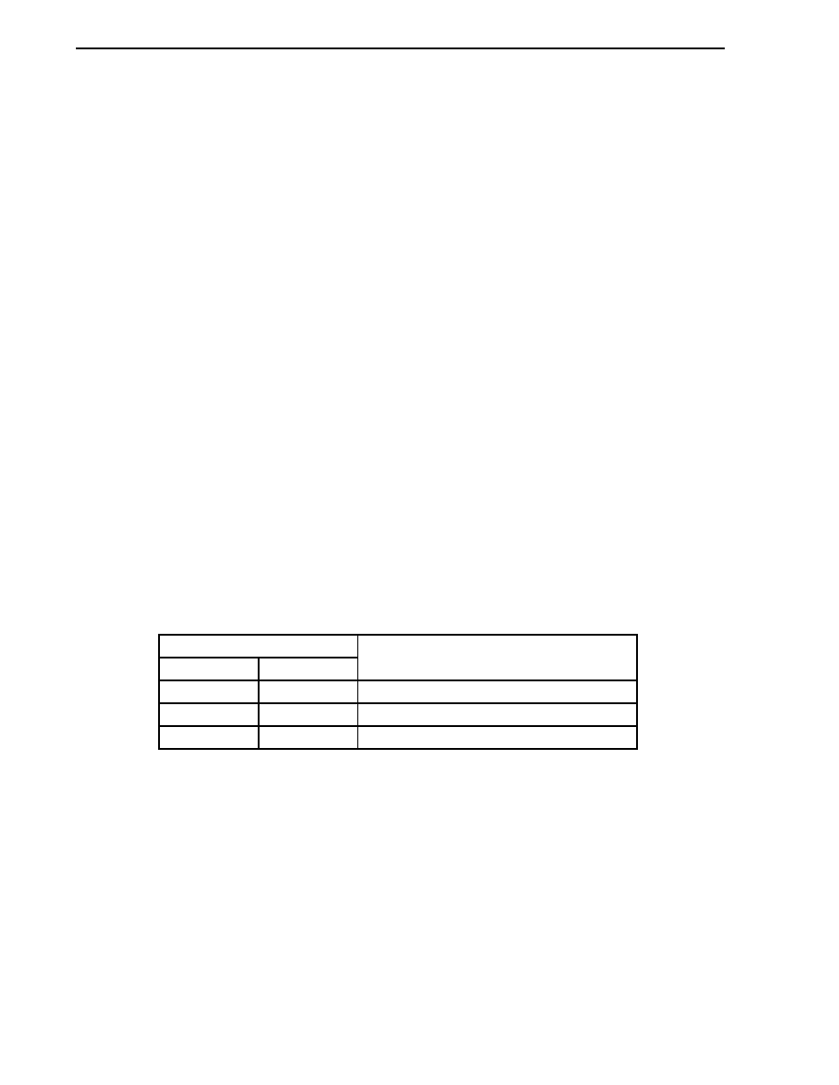
Operation When Reset Is Released
FLMD0
FLMD1
Operation Mode After Reset
L
×
Normal operation mode
H
L
Flash memory programming mode
H
Setting prohibited
Remark
L: Low-level input
H: High-level input
×: Don’t care
<R>
相關(guān)PDF資料 |
PDF描述 |
|---|---|
| UPD780031AYCW(A)-XXX | 8-BIT, MROM, 8.38 MHz, MICROCONTROLLER, PDIP64 |
| UPD780123GB(A1)-XXX-8ET | 8-BIT, MROM, 10 MHz, MICROCONTROLLER, PQFP52 |
| UPD780146GC-XXX-8BT | 8-BIT, MROM, 10 MHz, MICROCONTROLLER, PQFP80 |
| UPD784216AGC-XXX-8EU | 16-BIT, MROM, 12.5 MHz, MICROCONTROLLER, PQFP100 |
| UPD789304GK-XXX-9ET | 8-BIT, MROM, 5 MHz, MICROCONTROLLER, PQFP64 |
相關(guān)代理商/技術(shù)參數(shù) |
參數(shù)描述 |
|---|---|
| UPD70F3263GC-8EA-A | 制造商:Renesas Electronics Corporation 功能描述: |
| UPD70F3263HYGC-8EA-A | 制造商:Renesas Electronics Corporation 功能描述: |
| UPD70F3264YGJ-UEN-A | 制造商:Renesas Electronics Corporation 功能描述: |
| UPD70F3266YGJ-UEN-A | 制造商:Renesas Electronics Corporation 功能描述: |
| UPD70F3281YGC-8EA-A | 制造商:Renesas Electronics Corporation 功能描述: |
發(fā)布緊急采購(gòu),3分鐘左右您將得到回復(fù)。