- 您現(xiàn)在的位置:買賣IC網(wǎng) > PDF目錄98305 > TVP5020 (TEXAS INSTRUMENTS INC) COLOR SIGNAL DECODER, PQFP80 PDF資料下載
參數(shù)資料
| 型號: | TVP5020 |
| 廠商: | TEXAS INSTRUMENTS INC |
| 元件分類: | 顏色信號轉(zhuǎn)換 |
| 英文描述: | COLOR SIGNAL DECODER, PQFP80 |
| 封裝: | POWER, PLASTIC, TQFP-80 |
| 文件頁數(shù): | 40/89頁 |
| 文件大?。?/td> | 376K |
| 代理商: | TVP5020 |
第1頁第2頁第3頁第4頁第5頁第6頁第7頁第8頁第9頁第10頁第11頁第12頁第13頁第14頁第15頁第16頁第17頁第18頁第19頁第20頁第21頁第22頁第23頁第24頁第25頁第26頁第27頁第28頁第29頁第30頁第31頁第32頁第33頁第34頁第35頁第36頁第37頁第38頁第39頁當前第40頁第41頁第42頁第43頁第44頁第45頁第46頁第47頁第48頁第49頁第50頁第51頁第52頁第53頁第54頁第55頁第56頁第57頁第58頁第59頁第60頁第61頁第62頁第63頁第64頁第65頁第66頁第67頁第68頁第69頁第70頁第71頁第72頁第73頁第74頁第75頁第76頁第77頁第78頁第79頁第80頁第81頁第82頁第83頁第84頁第85頁第86頁第87頁第88頁第89頁
2–31
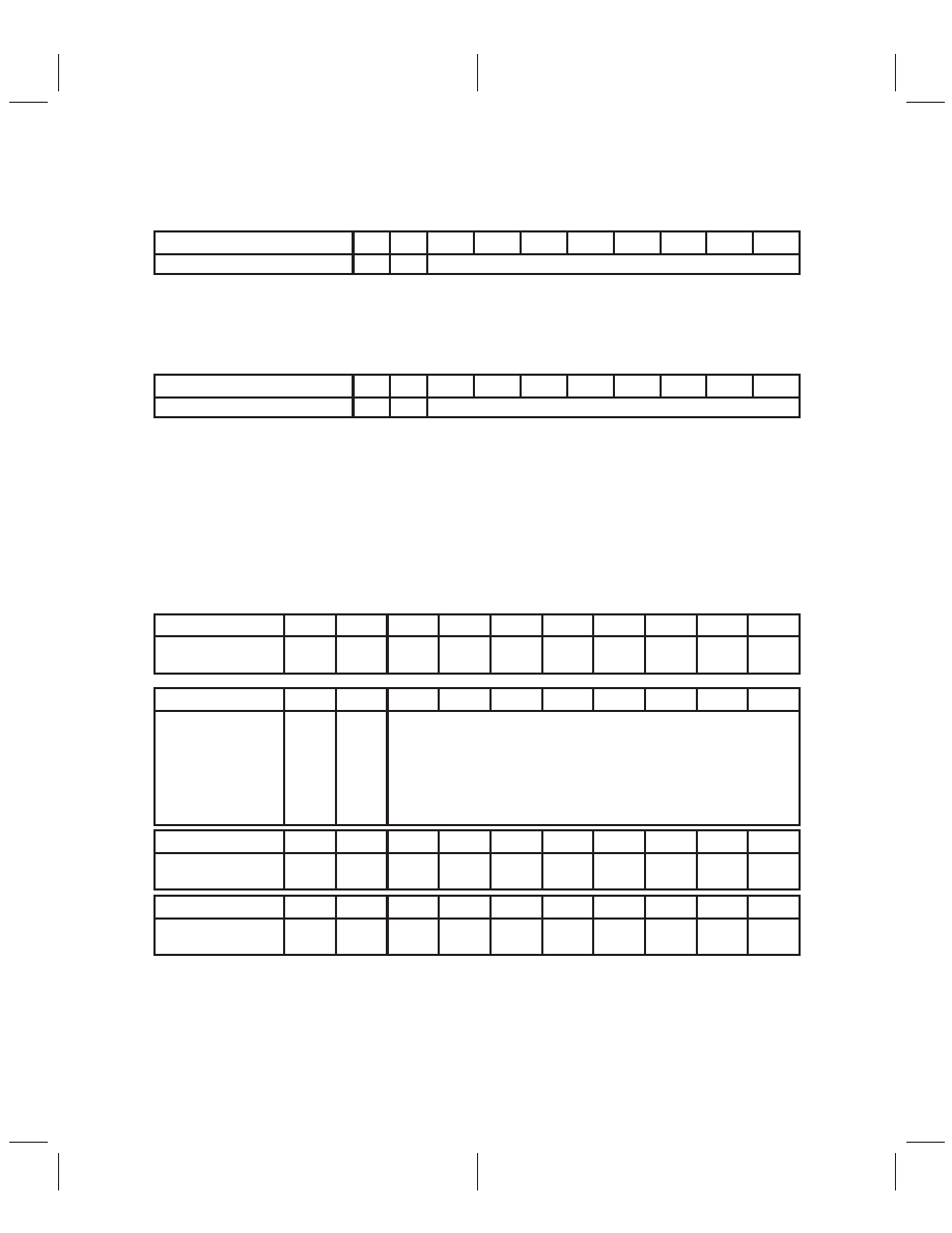
VBI FIFO:
The VBI FIFO containing sliced VBI data is directly readable by the VMI host.
A1
A0
D7
D6
D5
D4
D3
D2
D1
D0
Read VBI FIFO
1
0
Data from FIFO
Status/Interrupt Register:
The status/interrupt register provides the host with information containing the source of an interrupt. After
an interrupt condition is set, the condition can be reset by writing a one to the appropriate bit in the
status/interrupt register.
A1
A0
D7
D6
D5
D4
D3
D2
D1
D0
Access status/interrupt register
1
Data to/from status/interrupt register
2.11.2
VMI Microcode Write Operation
Data written to indirect register 7E will be written to the TVP5020 program RAM. During the address write
cycle the microprocessor resets and points to location zero in the program and remains reset. The
microprocessor requires a clear-reset operation upon completion of the write operation. The host performs
the reset by writing into the 7F register to clear reset and resume microprocessor function. (There is no
specific data to be written into the 7F register; any data will resume microprocessor function).
To avoid violating VMI cycle time requirements during microcode write operation, the host can poll the cycle
complete bit in the VMI status register after writing each byte of data to the VMI data register. Alternatively,
the cycle complete enable bit in the interrupt enable register (indirect address C1) can be set to generate
an interrupt for the host when a write operation is complete.
A1
A0
D7
D6
D5
D4
D3
D2
D1
D0
Write microcode
Register address
0
1
0
A1
A0
D7
D6
D5
D4
D3
D2
D1
D0
Write microcode
Register data
Write microcode
Register Data
Write microcode
Register data
0
1
First byte of microcode data
(Wait for cycle complete status or interrupt)
Second Byte of microcode data
(Wait for cycle complete status or interrupt)
Last byte of microcode data
(Wait for cycle complete status or interrupt)
A1
A0
D7
D6
D5
D4
D3
D2
D1
D0
Write clear reset
Register address
0
1
A1
A0
D7
D6
D5
D4
D3
D2
D1
D0
Write clear reset
Dummy data
0
1
X
相關(guān)PDF資料 |
PDF描述 |
|---|---|
| TVP5022 | COLOR SIGNAL DECODER, PQFP80 |
| TVP5031PFP | COLOR SIGNAL DECODER, PQFP80 |
| TVP5040CPFP | COLOR SIGNAL DECODER, PQFP80 |
| TVP5040PFP | COLOR SIGNAL DECODER, PQFP80 |
| TVP5041PFP | COLOR SIGNAL DECODER, PQFP80 |
相關(guān)代理商/技術(shù)參數(shù) |
參數(shù)描述 |
|---|---|
| TVP5020CPFP | 制造商:Rochester Electronics LLC 功能描述:- Bulk |
| TVP5020PFC | 制造商:未知廠家 制造商全稱:未知廠家 功能描述: |
| TVP5020TQFP | 制造商:TI 制造商全稱:Texas Instruments 功能描述:NTSC/PAL VIDEO DECODER |
| TVP5021PFP | 功能描述:視頻 IC NTSC/PAL DIGITAL VIDEO DECODER RoHS:否 制造商:Fairchild Semiconductor 工作電源電壓:5 V 電源電流:80 mA 最大工作溫度:+ 85 C 封裝 / 箱體:TSSOP-28 封裝:Reel |
| TVP5021PFPG4 | 功能描述:視頻 IC NTSC/PAL DIGITAL VIDEO DECODER RoHS:否 制造商:Fairchild Semiconductor 工作電源電壓:5 V 電源電流:80 mA 最大工作溫度:+ 85 C 封裝 / 箱體:TSSOP-28 封裝:Reel |
發(fā)布緊急采購,3分鐘左右您將得到回復。