- 您現(xiàn)在的位置:買賣IC網(wǎng) > PDF目錄98301 > TSA1401IFT (STMICROELECTRONICS) 1-CH 14-BIT PROPRIETARY METHOD ADC, PARALLEL ACCESS, PQFP48 PDF資料下載
參數(shù)資料
| 型號: | TSA1401IFT |
| 廠商: | STMICROELECTRONICS |
| 元件分類: | ADC |
| 英文描述: | 1-CH 14-BIT PROPRIETARY METHOD ADC, PARALLEL ACCESS, PQFP48 |
| 封裝: | 7 X 7 MM, TQFP-48 |
| 文件頁數(shù): | 4/19頁 |
| 文件大小: | 641K |
| 代理商: | TSA1401IFT |

Obsolete
Product(s)
- Obsolete
Product(s)
Obsolete
Product(s)
- Obsolete
Product(s)
TSA1401
APPLICATION INFORMATION
12/19
5
APPLICATION INFORMATION
The TSA1401 is a High Speed Analog to Digital
converter based on a pipeline architecture and the
latest deep sub micron CMOS process to achieve
the best performances in terms of linearity and
power consumption.
The pipeline structure consists of 14 internal
conversion stages in which the analog signal is
fed and sequentially converted into digital data.
Each of the 14 stages consists of an Analog to
Digital converter, a Digital to Analog converter, a
Sample and Hold and an amplifier (gain=2). A 1.5-
bit conversion resolution is achieved in each
stage. Each resulting LSB-MSB couple is then
time-shifted to recover from the delay caused by
conversion. Digital data correction completes the
processing by recovering from the redundancy of
the (LSB-MSB) couple for each stage. The
corrected data are outputted through the digital
buffers.
Signal input is sampled on the rising edge of the
clock while digital outputs are delivered on the
falling edge of the clock.
The advantages of such a converter reside in the
combination of pipeline architecture and the most
advanced technologies. The highest dynamic
performances are achieved while consumption
remains at the lowest level.
5.1 Analog Input Configuration
5.1.1 Analog input level and references
To maximize the TSA1401’s high-resolution and
speed, it is advisable to drive the analog input
differentially. The full scale of TSA1401 is
adjusted through the voltage value of VREFP and
VREFM:
VIN-VINB=2(VREFP-VREFM)
The
differential
analog
input
signal
always
presents a common mode voltage, CM:
CM=(VIN+VINB)/2
In order for the user to select the right full scale
according to the application, a control pin,
REFMODE, allows to switch from internal to
external references.
Internal references, common mode:
When REFMODE is set to VIL level, TSA1401
operates with its own reference voltage generated
by its internal bandgap. VREFM pin is connected
externally to the Analog Ground while VREFP is
set to its internal voltage (0.86V). The full scale of
the ADC when using internal references is 1.8Vpp
(to reduce the full scale if desired, VREFM may be
forced externally).
In this case VREFP and INCM are low impedance
outputs. INCM pin (voltage generator 0.46V) may
be used to supply the common mode, CM of the
analog input signal.
External references, common mode:
In applications requiring a different full scale
magnitude, it is possible to force externally
VREFP and INCM (REFM must be connected to
analog ground or forced externally).
REFMODE set to VIH level will put in standby
mode the internal references. In this case,
VREFP, INCM are high impedance inputs and
have
to
be
forced
by external
references.
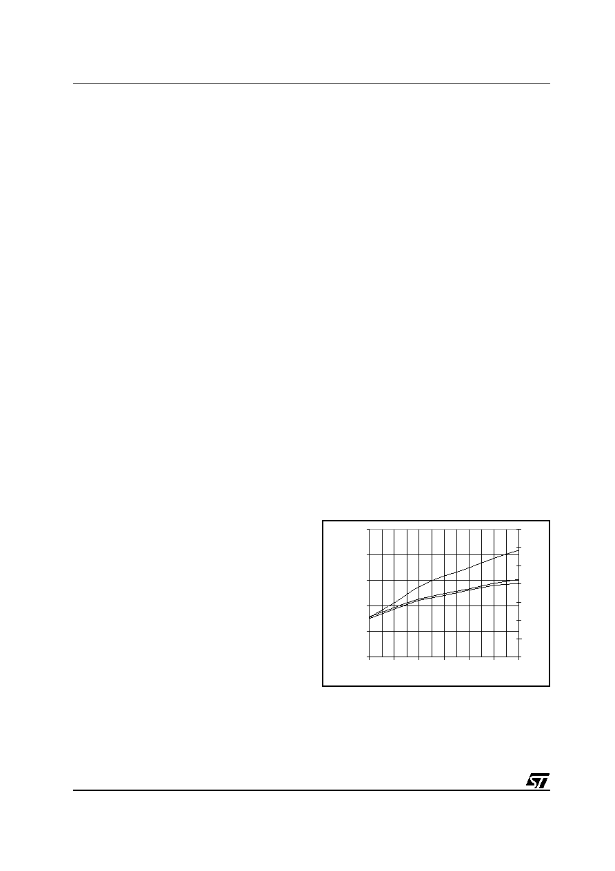
TSA1401 shows better performances when the
full scale is increased by the use of external
references (see
Fig. 10: Linearity vs. VREFP
Fin=5MHz;Fs=20Mhz;Icca=26mA;INCM=0.45V
65
68
71
74
77
80
0.8
0.9
1
1.1
1.2
1.3
1.4
REFP (V)
D
y
namic
par
a
met
e
rs
(
d
B
)
11
11.2
11.4
11.6
11.8
12
12.2
12.4
ENOB
SNR
SINAD
相關(guān)PDF資料 |
PDF描述 |
|---|---|
| TSA5522TD-T | PLL FREQUENCY SYNTHESIZER, 1400 MHz, PDSO16 |
| TSC2003IPWRQ1 | SPECIALTY CONSUMER CIRCUIT, PDSO16 |
| TSC2003IZQCT | 2-CH 12-BIT SUCCESSIVE APPROXIMATION ADC, SERIAL ACCESS, PBGA48 |
| TSC2003IPWT | 2-CH 12-BIT SUCCESSIVE APPROXIMATION ADC, SERIAL ACCESS, PDSO16 |
| TSC2003I | 3-CH 12-BIT SUCCESSIVE APPROXIMATION ADC, SERIAL ACCESS, PDSO16 |
相關(guān)代理商/技術(shù)參數(shù) |
參數(shù)描述 |
|---|---|
| TSA144C | 制造商:TSC 制造商全稱:Taiwan Semiconductor Company, Ltd 功能描述:PNP Digital Transistor |
| TSA144CCU | 制造商:TSC 制造商全稱:Taiwan Semiconductor Company, Ltd 功能描述:PNP Digital Transistor |
| TSA144CCX | 制造商:TSC 制造商全稱:Taiwan Semiconductor Company, Ltd 功能描述:PNP Digital Transistor |
| TSA15 | 制造商:未知廠家 制造商全稱:未知廠家 功能描述:EURO TERMINAL BLOCKS |
| TSA16 | 制造商:未知廠家 制造商全稱:未知廠家 功能描述:EURO TERMINAL BLOCKS |
發(fā)布緊急采購,3分鐘左右您將得到回復(fù)。