- 您現(xiàn)在的位置:買賣IC網(wǎng) > PDF目錄384021 > TMS28F004AMB70CDBJL (Texas Instruments, Inc.) 524288 BY 8-BIT/262144 BY 16-BIT AUTO-SELECT BOOT-BLOCK FLASH MEMORIES PDF資料下載
參數(shù)資料
| 型號: | TMS28F004AMB70CDBJL |
| 廠商: | Texas Instruments, Inc. |
| 英文描述: | 524288 BY 8-BIT/262144 BY 16-BIT AUTO-SELECT BOOT-BLOCK FLASH MEMORIES |
| 中文描述: | 524288按8-BIT/262144由16位自動選擇啟動塊閃存 |
| 文件頁數(shù): | 21/80頁 |
| 文件大?。?/td> | 1080K |
| 代理商: | TMS28F004AMB70CDBJL |
第1頁第2頁第3頁第4頁第5頁第6頁第7頁第8頁第9頁第10頁第11頁第12頁第13頁第14頁第15頁第16頁第17頁第18頁第19頁第20頁當(dāng)前第21頁第22頁第23頁第24頁第25頁第26頁第27頁第28頁第29頁第30頁第31頁第32頁第33頁第34頁第35頁第36頁第37頁第38頁第39頁第40頁第41頁第42頁第43頁第44頁第45頁第46頁第47頁第48頁第49頁第50頁第51頁第52頁第53頁第54頁第55頁第56頁第57頁第58頁第59頁第60頁第61頁第62頁第63頁第64頁第65頁第66頁第67頁第68頁第69頁第70頁第71頁第72頁第73頁第74頁第75頁第76頁第77頁第78頁第79頁第80頁
TMS28F004Axy, TMS28F400Axy
524288 BY 8-BIT/
262
144 BY 16-BIT
AUTO-SELECT BOOT-BLOCK FLASH MEMORIES
SMJS829A – JANUARY 1996 – REVISED AUGUST 1997
21
POST OFFICE BOX 1443
HOUSTON, TEXAS 77251–1443
absolute maximum ratings over operating free-air temperature range (unless otherwise noted)
Supply voltage range, V
CC
(see Note 4)
. . . . . . . . . . . . . . . . . . . . . . . . . . . . . . . . . . . . . . . . . . . . . .
Supply voltage range, V
PP
(see Note 4)
. . . . . . . . . . . . . . . . . . . . . . . . . . . . . . . . . . . . . . . . . . . . .
Input voltage range: All inputs except A9, RP
. . . . . . . . . . . . . . . . . . . . . . . . . . . . . . . . . . .
RP, A9 (see Note 5)
. . . . . . . . . . . . . . . . . . . . . . . . . . . . . . . . . . . . . . . . . .
Output voltage range (see Note 6)
. . . . . . . . . . . . . . . . . . . . . . . . . . . . . . . . . . . . . . . . . . . . .
Operating free-air temperature range, T
A
, during read/erase/program: L suffix
– 0.6 V to 7 V
– 0.6 V to 14 V
– 0.6 V to V
CC
+ 1 V
– 0.6 V to 13.5 V
– 0.6 V to V
CC
+ 1 V
0
°
C to 70
°
C
. . . . . . . . . . . . . .
– 40
°
C to 85
°
C
. . . . . . . . . . . .
– 40
°
C to 125
°
C
. . . . . . . . . .
– 65
°
C to 150
°
C
E suffix
Q suffix
Storage temperature range, T
stg
Stresses beyond those listed under “absolute maximum ratings” may cause permanent damage to the device. These are stress ratings only, and
functional operation of the device at these or any other conditions beyond those indicated under “recommended operating conditions” is not
implied. Exposure to absolute-maximum-rated conditions for extended periods may affect device reliability.
NOTES:
4. All voltage values are with respect to VSS.
5. The voltage on any input or output can undershoot to – 2 V for periods less than 20 ns. See Figure 8.
6. The voltage on any input or output can overshoot to 7 V for periods less than 20 ns. See Figure 9.
. . . . . . . . . . . . . . . . . . . . . . . . . . . . . . . . . . . . . . . . . . . . . . . . . .
IOL
IOH
Output
Under
Test
CL
(see Note A)
VZ
VIH
VOLTAGE WAVEFORMS
VIL
VOH
VOL
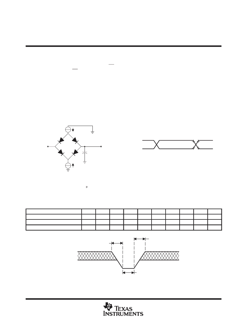
NOTES: A. CL includes probe and fixture capacitance.
B. AC test conditions are driven at VIH and VIL, Timing measurements are made at VOH and VOL levels on both inputs and outputs.
See Table 9 for values based on VCC operating range..
C. Each device must have a 0.1 F ceramic capacitor connected to VCC and VSS as close as possible to the device pins.
Figure 7. Load Circuit and Voltage Waveforms
Table 9. AC Test Conditions
VCC RANGE
5 V
±
10%
3.3
±
0.3 V
2.7 to 3.6 V
IOL
2.1
IOH
–0.4
VZ
1.5
VOL
0.8
VOH
2.0
VIL
0.45
VIH
2.4
CL
100
tf
tr
< 10
< 10
0.5
–0.5
1.5
1.5
1.5
0.0
3.0
50
< 10
< 10
0.1
–0.1
1.35
1.35
1.35
0.0
2.7
50
< 10
< 10
VZ is the measured value used to detect high impedance.
– 2.0 V
–0.6 V
+0.8 V
5 ns
5 ns
20 ns
Figure 8. Maximum Negative Overshoot Waveform
相關(guān)PDF資料 |
PDF描述 |
|---|---|
| TMS320AV110 | MPEG Audio Decoder(MPEG音頻譯碼器) |
| TMS320AV120 | MPEG Audio Decoder(MPEG音頻譯碼器) |
| TMS320AV220 | Video CD MPEG Decoder(視頻CD MPEG編碼器) |
| TMS320AV410 | Digital NTSC/PAL Encoder(數(shù)字NTSC/PAL編碼器) |
| TMS320AV411 | Digital NTSC/PAL Encoder(數(shù)字NTSC/PAL編碼器) |
相關(guān)代理商/技術(shù)參數(shù) |
參數(shù)描述 |
|---|---|
| TMS28F004AMB70CDCDE | 制造商:未知廠家 制造商全稱:未知廠家 功能描述:x8 Flash EEPROM |
| TMS28F004AMB70CDCDL | 制造商:未知廠家 制造商全稱:未知廠家 功能描述:x8 Flash EEPROM |
| TMS28F004AMB80BDBJL | 制造商:TI 制造商全稱:Texas Instruments 功能描述:524288 BY 8-BIT/262144 BY 16-BIT AUTO-SELECT BOOT-BLOCK FLASH MEMORIES |
| TMS28F004AMB80BDCDE | 制造商:未知廠家 制造商全稱:未知廠家 功能描述:x8 Flash EEPROM |
| TMS28F004AMB80BDCDL | 制造商:未知廠家 制造商全稱:未知廠家 功能描述:x8 Flash EEPROM |
發(fā)布緊急采購,3分鐘左右您將得到回復(fù)。