- 您現(xiàn)在的位置:買賣IC網(wǎng) > PDF目錄384021 > TMS28F004AMB60CDBJL (Texas Instruments, Inc.) 524288 BY 8-BIT/262144 BY 16-BIT AUTO-SELECT BOOT-BLOCK FLASH MEMORIES PDF資料下載
參數(shù)資料
| 型號(hào): | TMS28F004AMB60CDBJL |
| 廠商: | Texas Instruments, Inc. |
| 英文描述: | 524288 BY 8-BIT/262144 BY 16-BIT AUTO-SELECT BOOT-BLOCK FLASH MEMORIES |
| 中文描述: | 524288按8-BIT/262144由16位自動(dòng)選擇啟動(dòng)塊閃存 |
| 文件頁數(shù): | 10/80頁 |
| 文件大小: | 1080K |
| 代理商: | TMS28F004AMB60CDBJL |
第1頁第2頁第3頁第4頁第5頁第6頁第7頁第8頁第9頁當(dāng)前第10頁第11頁第12頁第13頁第14頁第15頁第16頁第17頁第18頁第19頁第20頁第21頁第22頁第23頁第24頁第25頁第26頁第27頁第28頁第29頁第30頁第31頁第32頁第33頁第34頁第35頁第36頁第37頁第38頁第39頁第40頁第41頁第42頁第43頁第44頁第45頁第46頁第47頁第48頁第49頁第50頁第51頁第52頁第53頁第54頁第55頁第56頁第57頁第58頁第59頁第60頁第61頁第62頁第63頁第64頁第65頁第66頁第67頁第68頁第69頁第70頁第71頁第72頁第73頁第74頁第75頁第76頁第77頁第78頁第79頁第80頁
TMS28F004Axy, TMS28F400Axy
524288 BY 8-BIT/
262
144 BY 16-BIT
AUTO-SELECT BOOT-BLOCK FLASH MEMORIES
SMJS829A – JANUARY 1996 – REVISED AUGUST 1997
10
POST OFFICE BOX 1443
HOUSTON, TEXAS 77251–1443
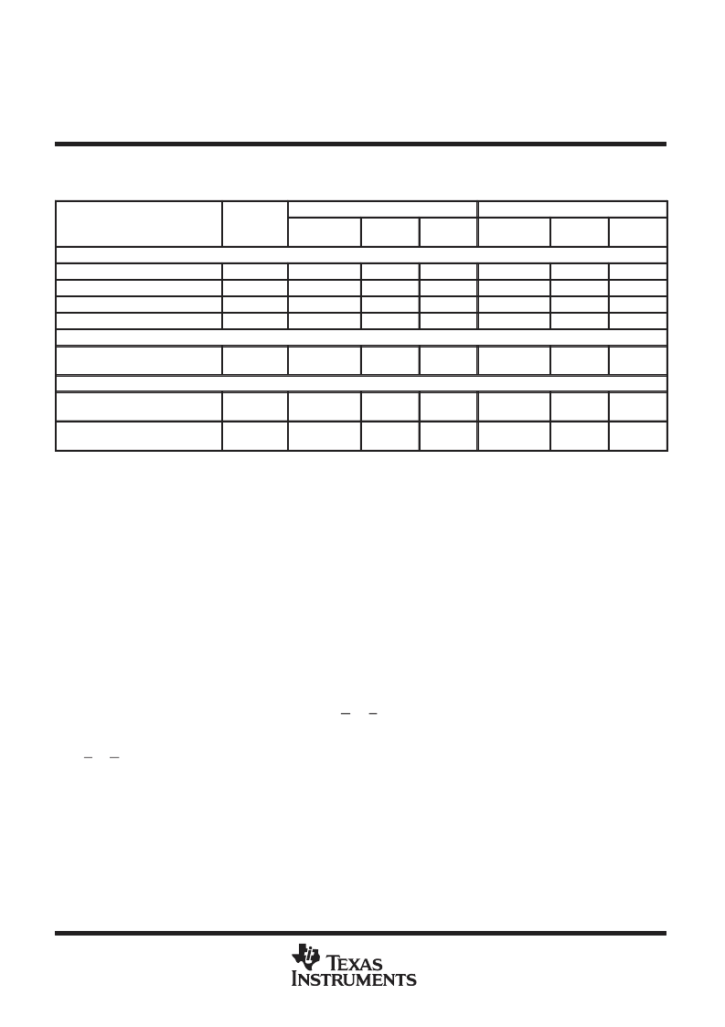
command definitions (continued)
Table 4. Command Definitions
BUS
CYCLES
REQUIRED
FIRST BUS CYCLE
SECOND BUS CYCLE
COMMAND
OPERATION
ADDRESS
CSM
INPUT
OPERATION
ADDRESS
DATA
IN/OUT
Read Operations
Read Array
1
Write
X
FFh
Read
X
Data Out
Read Algorithm-Selection Code
2
Write
X
90h
Read
A0
M/D
Read-Status Register
2
Write
X
70h
Read
X
SRB
Clear-Status Register
1
Write
X
50h
Program Mode
Program Setup/Program
(byte/word)
2
Write
PA
40h or 10h
Write
PA
PD
Erase Operations
Block-Erase Setup/
Block-Erase Confirm
2
Write
BEA
20h
Write
BEA
D0h
Erase Suspend/
Erase Resume
2
Write
X
B0h
Write
X
D0h
Legend:
BEA
M/D
PA
PD
SRB
X
Block-erase address. Any address selected within a block selects that block for erase.
Manufacturer-equivalent/device-equivalent code
Address to be programmed
Data to be programmed at PA
Status-register data byte that can be found on DQ0–DQ7
Don’t care
status register
The status register allows the user to determine whether the state of a program/erase operation is pending or
complete. The status register is monitored by writing a read-status command to the CSM and reading the
resulting status code on I/O pins DQ0–DQ7. This is valid for operation in either the byte- or word-wide mode.
When writing to the CSM in word-wide mode, the high order I/O pins (DQ8–DQ15) can be set to any valid 2-state
level. When reading the status bits during a word-wide read operation, the high order I/Os (DQ8–DQ15) are
set to 00h internally, so the user needs to interpret only the low order I/O pins (D0–DQ7).
After a read-status command has been given, the data appearing on DQ0–DQ7 remains as status register data
until a new command is issued to the CSM. To return the device to other modes of operation, a new command
must be issued to the CSM.
Register data is updated on the falling edge of G or E. The latest falling edge of either of these two signals
updates the latch within a given read cycle. Latching the data prevents errors from occurring if the register input
change during a status-register read. To ensure that the status-register output contains updated status data,
E or G must be toggled for each subsequent status read.
The status register provides the internal state of the WSM to the external microprocessor. During periods when
the WSM is active, the status register can be polled to determine the WSM status. Table 5 defines the status
register bits and their functions.
相關(guān)PDF資料 |
PDF描述 |
|---|---|
| TMS28F004AMB70BDBJL | 524288 BY 8-BIT/262144 BY 16-BIT AUTO-SELECT BOOT-BLOCK FLASH MEMORIES |
| TMS28F004AMB70CDBJL | 524288 BY 8-BIT/262144 BY 16-BIT AUTO-SELECT BOOT-BLOCK FLASH MEMORIES |
| TMS320AV110 | MPEG Audio Decoder(MPEG音頻譯碼器) |
| TMS320AV120 | MPEG Audio Decoder(MPEG音頻譯碼器) |
| TMS320AV220 | Video CD MPEG Decoder(視頻CD MPEG編碼器) |
相關(guān)代理商/技術(shù)參數(shù) |
參數(shù)描述 |
|---|---|
| TMS28F004AMB60CDCDE | 制造商:未知廠家 制造商全稱:未知廠家 功能描述:x8 Flash EEPROM |
| TMS28F004AMB60CDCDL | 制造商:未知廠家 制造商全稱:未知廠家 功能描述:x8 Flash EEPROM |
| TMS28F004AMB70BDBJL | 制造商:TI 制造商全稱:Texas Instruments 功能描述:524288 BY 8-BIT/262144 BY 16-BIT AUTO-SELECT BOOT-BLOCK FLASH MEMORIES |
| TMS28F004AMB70BDCDE | 制造商:未知廠家 制造商全稱:未知廠家 功能描述:x8 Flash EEPROM |
| TMS28F004AMB70BDCDL | 制造商:未知廠家 制造商全稱:未知廠家 功能描述:x8 Flash EEPROM |
發(fā)布緊急采購,3分鐘左右您將得到回復(fù)。