- 您現(xiàn)在的位置:買賣IC網(wǎng) > PDF目錄384024 > TMP320C6205GHKA200 (Texas Instruments, Inc.) FIXED-POINT DIGITAL SIGNAL PROCESSOR PDF資料下載
參數(shù)資料
| 型號(hào): | TMP320C6205GHKA200 |
| 廠商: | Texas Instruments, Inc. |
| 元件分類: | 數(shù)字信號(hào)處理 |
| 英文描述: | FIXED-POINT DIGITAL SIGNAL PROCESSOR |
| 中文描述: | 定點(diǎn)數(shù)字信號(hào)處理器 |
| 文件頁(yè)數(shù): | 48/72頁(yè) |
| 文件大小: | 1143K |
| 代理商: | TMP320C6205GHKA200 |
第1頁(yè)第2頁(yè)第3頁(yè)第4頁(yè)第5頁(yè)第6頁(yè)第7頁(yè)第8頁(yè)第9頁(yè)第10頁(yè)第11頁(yè)第12頁(yè)第13頁(yè)第14頁(yè)第15頁(yè)第16頁(yè)第17頁(yè)第18頁(yè)第19頁(yè)第20頁(yè)第21頁(yè)第22頁(yè)第23頁(yè)第24頁(yè)第25頁(yè)第26頁(yè)第27頁(yè)第28頁(yè)第29頁(yè)第30頁(yè)第31頁(yè)第32頁(yè)第33頁(yè)第34頁(yè)第35頁(yè)第36頁(yè)第37頁(yè)第38頁(yè)第39頁(yè)第40頁(yè)第41頁(yè)第42頁(yè)第43頁(yè)第44頁(yè)第45頁(yè)第46頁(yè)第47頁(yè)當(dāng)前第48頁(yè)第49頁(yè)第50頁(yè)第51頁(yè)第52頁(yè)第53頁(yè)第54頁(yè)第55頁(yè)第56頁(yè)第57頁(yè)第58頁(yè)第59頁(yè)第60頁(yè)第61頁(yè)第62頁(yè)第63頁(yè)第64頁(yè)第65頁(yè)第66頁(yè)第67頁(yè)第68頁(yè)第69頁(yè)第70頁(yè)第71頁(yè)第72頁(yè)
SPRS106G OCTOBER 1999 REVISED JULY 2006
48
POST OFFICE BOX 1443
HOUSTON, TEXAS 772511443
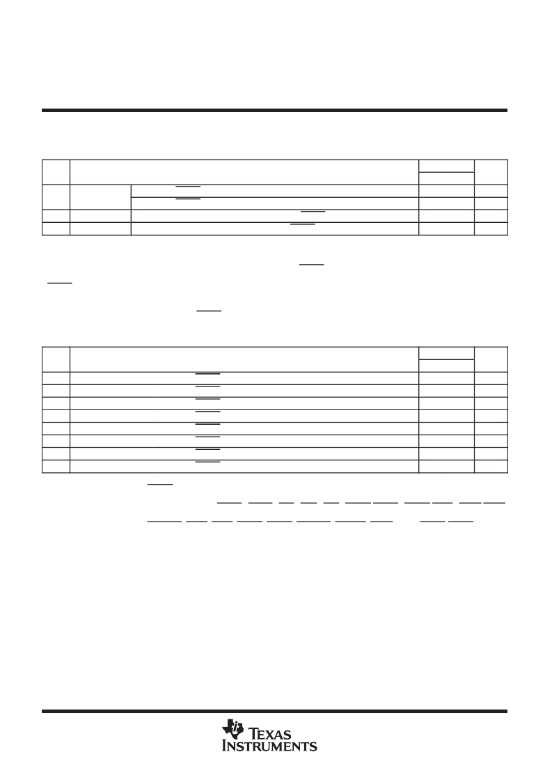
RESET TIMING
timing requirements for reset (see Figure 28)
NO.
200
UNIT
MIN
10P
MAX
1
tw(RST)
Width of the RESET pulse (PLL stable)
Width of the RESET pulse (PLL needs to sync up)§
Setup time, ED boot configuration bits valid before RESET high
Hold time, ED boot configuration bits valid after RESET high
This parameter applies to CLKMODE x1 when CLKIN is stable, and applies to CLKMODE x4, x6, x7, x8, x9, x10, and x11 when CLKIN and PLL
are stable.
P = 1/CPU clock frequency in ns. For example, when running parts at 200 MHz, use P = 5 ns.
§This parameter applies to CLKMODE x4, x6, x7, x8, x9, x10, and x11 only. The RESET signal is not connected internally to the Clock PLL circuit.
The PLL requires a minimum of 250
μ
s to stabilize following device power up or after PLL configuration has been changed. During that time,
RESET must be asserted to ensure proper device operation. See the
clock PLL
section for power up (specifically Figure 5, Note E) and for PLL
lock times (Table 4).
ED[31:0] are the boot configuration pins during device reset.
#A 250
μ
s setup time before the rising edge of RESET is required when using CLKMODE x4, x6, x7, x8, x9, x10, or x11.
ns
μ
s
ns
250
5P#
5P
10
tsu(ED)
th(ED)
11
ns
switching characteristics over recommended operating conditions during reset
||
(see Figure 28)
NO.
PARAMETER
200
UNIT
MIN
MAX
2
td(RSTL-CKO2IV)
td(RSTH-CKO2V)
td(RSTL-HIGHIV)
td(RSTH-HIGHV)
td(RSTL-LOWIV)
td(RSTH-LOWV)
td(RSTL-ZHZ)
td(RSTH-ZV)
Delay time, RESET low to CLKOUT2 invalid
P
ns
3
Delay time, RESET high to CLKOUT2 valid
4P
ns
4
Delay time, RESET low to high group invalid
P
ns
5
Delay time, RESET high to high group valid
4P
ns
6
Delay time, RESET low to low group invalid
P
ns
7
Delay time, RESET high to low group valid
4P
ns
8
Delay time, RESET low to Z group high impedance
P
ns
9
Delay time, RESET high to Z group valid
4P
ns
P = 1/CPU clock frequency in ns. For example, when running parts at 200 MHz, use P = 5 ns.
||High group consists of:
HOLDA
Low group consists of:
IACK, INUM[3:0], DMAC[3:0], PD, TOUT0, and TOUT1, XSP_CLK, XSP_DO, and XSP_CS
Z group consists of:
EA[21:2], ED[31:0], CE[3:0], BE[3:0], ARE, AWE, AOE, SDCAS/SSADS, SDRAS/SSOE, SDWE/SSWE,
SDA10, CLKX0, CLKX1, FSX0, FSX1, DX0, DX1, CLKR0, CLKR1, FSR0, FSR1, AD[31:0],
PCBE[3:0], PINTA, PREQ, PSERR, PPERR, PDEVSEL, PFRAME, PIRDY, PPAR, PSTOP, PTRDY, and PME
相關(guān)PDF資料 |
PDF描述 |
|---|---|
| TMP320C6205ZHK200 | FIXED-POINT DIGITAL SIGNAL PROCESSOR |
| TMP320C6205ZHKA200 | FIXED-POINT DIGITAL SIGNAL PROCESSOR |
| TMX320DM6446ZWT | Digital Media System on-Chip |
| TN28F010-90 | 28F010 1024K (128K X 8) CMOS FLASH MEMORY |
| TN28F010-120 | 28F010 1024K (128K X 8) CMOS FLASH MEMORY |
相關(guān)代理商/技術(shù)參數(shù) |
參數(shù)描述 |
|---|---|
| TMP320C6205GJC100 | 制造商:TI 制造商全稱:Texas Instruments 功能描述:FIXED-POINT DIGITAL SIGNAL PROCESSOR |
| TMP320C6205GJC120 | 制造商:TI 制造商全稱:Texas Instruments 功能描述:FIXED-POINT DIGITAL SIGNAL PROCESSOR |
| TMP320C6205GJCA100 | 制造商:TI 制造商全稱:Texas Instruments 功能描述:FIXED-POINT DIGITAL SIGNAL PROCESSOR |
| TMP320C6205GJL100 | 制造商:TI 制造商全稱:Texas Instruments 功能描述:FIXED-POINT DIGITAL SIGNAL PROCESSOR |
| TMP320C6205GJL120 | 制造商:TI 制造商全稱:Texas Instruments 功能描述:FIXED-POINT DIGITAL SIGNAL PROCESSOR |
發(fā)布緊急采購(gòu),3分鐘左右您將得到回復(fù)。