- 您現(xiàn)在的位置:買賣IC網(wǎng) > PDF目錄383956 > TLV1543M (Texas Instruments, Inc.) 3.3-V 10-BIT ANALOG-TO-DIGITAL CONVERTERS WITH SERIAL CONTROL AND 11 ANALOG INPUTS PDF資料下載
參數(shù)資料
| 型號(hào): | TLV1543M |
| 廠商: | Texas Instruments, Inc. |
| 英文描述: | 3.3-V 10-BIT ANALOG-TO-DIGITAL CONVERTERS WITH SERIAL CONTROL AND 11 ANALOG INPUTS |
| 中文描述: | 3.3 V的10位模擬數(shù)字轉(zhuǎn)換器與串行控制和11個(gè)模擬輸入 |
| 文件頁數(shù): | 7/18頁 |
| 文件大?。?/td> | 295K |
| 代理商: | TLV1543M |
TLV1543C, TLV1543M
3.3-V 10-BIT ANALOG-TO-DIGITAL CONVERTERS
WITH SERIAL CONTROL AND 11 ANALOG INPUTS
SLAS072C – DECEMBER 1992 – REVISED MARCH 1995
7
POST OFFICE BOX 655303
DALLAS, TEXAS 75265
converter and analog input (continued)
SC
Threshold
Detector
Node 512
REF–
REF+
ST
512
VI
To Output
Latches
REF–
ST
REF+
REF–
ST
REF+
REF–
ST
REF+
REF–
ST
REF+
REF–
ST
REF+
REF–
ST
REF+
REF–
ST
REF–
ST
1
1
2
4
8
16
128
256
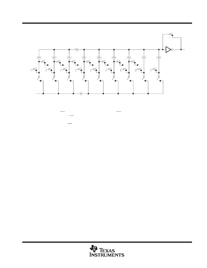
Figure 1. Simplified Model of the Successive-Approximation System
chip-select operation
The trailing edge of CS starts all modes of operation, and CS can abort a conversion sequence in any mode.
A high-to-low transition on CS within the specified time during an ongoing cycle aborts the cycle, and the device
returns to the initial state (the contents of the output data register remain at the previous conversion result).
Exercise care to prevent CS from being taken low close to completion of conversion because the output data
can be corrupted.
reference voltage inputs
There are two reference inputs used with these devices: REF+ and REF–. These voltage values establish the
upper and lower limits of the analog input to produce a full-scale and zero-scale reading respectively. The values
of REF+, REF–, and the analog input should not exceed the positive supply or be lower than GND consistent
with the specified absolute maximum ratings. The digital output is at full scale when the input signal is equal
to or higher than REF+ and at zero when the input signal is equal to or lower than REF–.
absolute maximum ratings over operating free-air temperature range (unless otherwise noted)
Supply voltage range, V
CC
(see Note 1): TLV1543C
–0.5 V to 6.5 V
–0.5 V to 6 V
–0.3 V to V
CC
+ 0.3 V
–0.3 V to V
CC
+ 0.3 V
V
CC
+ 0.1 V
. . . . . . . . . . . . . . . . . . . . . . . . . . . . . . . . . . .
. . . . . . . . . . . . . . . . . . . . . . . . . . . . . . . . . . . .
. . . . . . . . . . . . . . . . . . . . . . . . . . . . . . . . . . . . . . . . . . . .
. . . . . . . . . . . . . . . . . . . . . . . . . . . . . . . . . . . . . . . . . . . . . . . . . . .
Positive reference voltage, V
ref+
. . . . . . . . . . . . . . . . . . . . . . . . . . . . . . . . . . . . . . . . . . . . . . . . . . . . . .
Negative reference voltage, V
ref–
. . . . . . . . . . . . . . . . . . . . . . . . . . . . . . . . . . . . . . . . . . . . . . . . . . . . . . . . . .
Peak input current (any input)
. . . . . . . . . . . . . . . . . . . . . . . . . . . . . . . . . . . . . . . . . . . . . . . . . . . . . . . . . . . .
Peak total input current (all inputs)
. . . . . . . . . . . . . . . . . . . . . . . . . . . . . . . . . . . . . . . . . . . . . . . . . . . . . . . .
Operating free-air temperature range, T
A
: TLV1543C
TLV1543M
Storage temperature range, T
stg
. . . . . . . . . . . . . . . . . . . . . . . . . . . . . . . . . . . . . . . . . . . . . . . . . . .
Lead temperature 1,6 mm (1/16 inch) from the case for 10 seconds
Stresses beyond those listed under “absolute maximum ratings” may cause permanent damage to the device. These are stress ratings only, and
functional operation of the device at these or any other conditions beyond those indicated under “recommended operating conditions” is not
implied. Exposure to absolute-maximum-rated conditions for extended periods may affect device reliability.
NOTE 1: All voltage values are with respect to digital ground with REF– and GND wired together (unless otherwise noted).
TLV1543M
Input voltage range, V
I
(any input)
Output voltage range, V
O
–0.1 V
±
20 mA
±
30 mA
0
°
C to 70
°
C
–55
°
C to 125
°
C
–65
°
C to 150
°
C
. . . . . . . . . . . . . . . . . . . . . . . . . . . . . . . . . . . .
. . . . . . . . . . . . . . . . . . . . . . . . . . . . . . . . .
260
°
C
. . . . . . . . . . . . . . . . . . . . . . . . . . . .
相關(guān)PDF資料 |
PDF描述 |
|---|---|
| TLV1543MFK | 3.3-V 10-BIT ANALOG-TO-DIGITAL CONVERTERS WITH SERIAL CONTROL AND 11 ANALOG INPUTS |
| TLV1549C | 10-BIT ANALOG-TO-DIGITAL CONVERTERS WITH SERIAL CONTROL |
| TLV1549M | Standoff; Spacing Height:1"; Spacer Style:Hex; Spacer Thread Type:Female / Female; Spacer Material:Aluminum; Thread Size:6-32; Body Diameter:0.25" RoHS Compliant: Yes |
| TLV1549MFK | 10-BIT ANALOG-TO-DIGITAL CONVERTERS WITH SERIAL CONTROL |
| TLV1549MJG | 10-BIT ANALOG-TO-DIGITAL CONVERTERS WITH SERIAL CONTROL |
相關(guān)代理商/技術(shù)參數(shù) |
參數(shù)描述 |
|---|---|
| TLV1543MFK | 制造商:TI 制造商全稱:Texas Instruments 功能描述:3.3V 10 BIT ANALOG TO DIGITAL CONVERTERS WITH SERIAL CONTROL AND 11 ANALOG INPUTS |
| TLV1543MFKB | 制造商:Rochester Electronics LLC 功能描述:- Bulk |
| TLV1543MJ | 制造商:TI 制造商全稱:Texas Instruments 功能描述:3.3V 10 BIT ANALOG TO DIGITAL CONVERTERS WITH SERIAL CONTROL AND 11 ANALOG INPUTS |
| TLV1543MJB | 制造商:TI 制造商全稱:Texas Instruments 功能描述:3.3V 10 BIT ANALOG TO DIGITAL CONVERTERS WITH SERIAL CONTROL AND 11 ANALOG INPUTS |
| TLV1544 | 制造商:TI 制造商全稱:Texas Instruments 功能描述:LOW-VOLTAGE 10-BIT ANALOG-TO-DIGITAL CONVERTERS WITH SERIAL CONTROL AND 4/8 ANALOG INPUTS |
發(fā)布緊急采購,3分鐘左右您將得到回復(fù)。