- 您現(xiàn)在的位置:買賣IC網(wǎng) > PDF目錄383996 > THS4031DGN (Texas Instruments, Inc.) 100-MHz LOW-NOISE HIGH-SPEED AMPLIFIERS PDF資料下載
參數(shù)資料
| 型號: | THS4031DGN |
| 廠商: | Texas Instruments, Inc. |
| 英文描述: | 100-MHz LOW-NOISE HIGH-SPEED AMPLIFIERS |
| 中文描述: | 100 MHz的低噪聲高速放大器 |
| 文件頁數(shù): | 29/38頁 |
| 文件大?。?/td> | 674K |
| 代理商: | THS4031DGN |
第1頁第2頁第3頁第4頁第5頁第6頁第7頁第8頁第9頁第10頁第11頁第12頁第13頁第14頁第15頁第16頁第17頁第18頁第19頁第20頁第21頁第22頁第23頁第24頁第25頁第26頁第27頁第28頁當(dāng)前第29頁第30頁第31頁第32頁第33頁第34頁第35頁第36頁第37頁第38頁
THS4031, THS4032
100-MHz LOW-NOISE HIGH-SPEED AMPLIFIERS
SLOS224C – JULY 1999 – REVISED APRIL 2000
29
POST OFFICE BOX 655303
DALLAS, TEXAS 75265
APPLICATION INFORMATION
general PowerPAD
design considerations (continued)
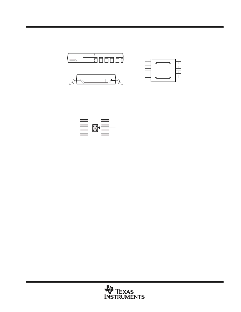
DIE
Side View (a)
End View (b)
Bottom View (c)
DIE
Thermal
Pad
NOTE B: The thermal pad is electrically isolated from all terminals in the package.
Figure 54. Views of Thermally Enhanced DGN Package
Although there are many ways to properly heatsink this device, the following steps illustrate the recommended
approach.
Thermal pad area (68 mils x 70 mils) with 5 vias
(Via diameter = 13 mils)
Figure 55. PowerPAD
PCB Etch and Via Pattern
1.
Prepare the PCB with a top-side etch pattern as shown in Figure 55. There should be etch for the leads as
well as etch for the thermal pad.
2.
Place five holes in the area of the thermal pad. These holes should be 13 mils in diameter. They are kept
small so that solder wicking through the holes is not a problem during reflow.
3.
Additional vias may be placed anywhere along the thermal plane outside of the thermal pad area. This helps
dissipate the heat generated by the THS403xDGN IC. These additional vias may be larger than the 13-mil
diameter vias directly under the thermal pad. They can be larger because they are not in the thermal pad
area to be soldered so that wicking is not a problem.
4.
Connect all holes to the internal ground plane.
5.
When connecting these holes to the ground plane, do
notuse the typical web or spoke via connection
methodology. Web connections have a high thermal-resistance connection that is useful for slowing the
heat transfer during soldering operations. This makes the soldering of vias that have plane connections
easier. In this application, however, low thermal resistance is desired for the most efficient heat transfer.
Therefore, the holes under the THS403xDGN package should connect to the internal ground plane with a
complete connection around the entire circumference of the plated-through hole.
6.
The top-side solder mask should leave the terminals of the package and the thermal pad area with its five
holes exposed. The bottom-side solder mask should cover the five holes of the thermal pad area, which
prevents solder from being pulled away from the thermal pad area during the reflow process.
7.
Apply solder paste to the exposed thermal pad area and to all the IC terminals.
8.
With these preparatory steps in place, the THS403xDGN IC is simply placed in position and run through
the solder reflow operation as any standard surface-mount component. This results in a part that is properly
installed.
相關(guān)PDF資料 |
PDF描述 |
|---|---|
| THS4031EVM | 100-MHz LOW-NOISE HIGH-SPEED AMPLIFIERS |
| THS4031FK | 100-MHz LOW-NOISE HIGH-SPEED AMPLIFIERS |
| THS4031MFK | 100-MHz LOW-NOISE HIGH-SPEED AMPLIFIERS |
| THS4032D | 100-MHz LOW-NOISE HIGH-SPEED AMPLIFIERS |
| THS4032DGN | 100-MHz LOW-NOISE HIGH-SPEED AMPLIFIERS |
相關(guān)代理商/技術(shù)參數(shù) |
參數(shù)描述 |
|---|---|
| THS4031-EP | 制造商:TI 制造商全稱:Texas Instruments 功能描述:100-MHz LOW-NOISE HIGH-SPEED AMPLIFIERS |
| THS4031EVM | 功能描述:放大器 IC 開發(fā)工具 THS4031 Hi-Spd Amp Eval Mod RoHS:否 制造商:International Rectifier 產(chǎn)品:Demonstration Boards 類型:Power Amplifiers 工具用于評估:IR4302 工作電源電壓:13 V to 23 V |
| THS4031FK | 制造商:TI 制造商全稱:Texas Instruments 功能描述:100-MHz LOW-NOISE HIGH-SPEED AMPLIFIERS |
| THS4031ID | 功能描述:高速運算放大器 100MHz Low Noise RoHS:否 制造商:Texas Instruments 通道數(shù)量:1 電壓增益 dB:116 dB 輸入補償電壓:0.5 mV 轉(zhuǎn)換速度:55 V/us 工作電源電壓:36 V 電源電流:7.5 mA 最大工作溫度:+ 85 C 安裝風(fēng)格:SMD/SMT 封裝 / 箱體:SOIC-8 封裝:Tube |
| THS4031IDG4 | 功能描述:高速運算放大器 100-MHz Low Noise Volt-Feedback Amp RoHS:否 制造商:Texas Instruments 通道數(shù)量:1 電壓增益 dB:116 dB 輸入補償電壓:0.5 mV 轉(zhuǎn)換速度:55 V/us 工作電源電壓:36 V 電源電流:7.5 mA 最大工作溫度:+ 85 C 安裝風(fēng)格:SMD/SMT 封裝 / 箱體:SOIC-8 封裝:Tube |
發(fā)布緊急采購,3分鐘左右您將得到回復(fù)。