- 您現(xiàn)在的位置:買賣IC網(wǎng) > PDF目錄98141 > SPL505YC264BT 400 MHz, PROC SPECIFIC CLOCK GENERATOR, PDSO64 PDF資料下載
參數(shù)資料
| 型號: | SPL505YC264BT |
| 元件分類: | 時(shí)鐘產(chǎn)生/分配 |
| 英文描述: | 400 MHz, PROC SPECIFIC CLOCK GENERATOR, PDSO64 |
| 封裝: | 6 X 17 MM, LEAD FREE, MO-153, TSSOP-64 |
| 文件頁數(shù): | 12/27頁 |
| 文件大小: | 314K |
| 代理商: | SPL505YC264BT |
第1頁第2頁第3頁第4頁第5頁第6頁第7頁第8頁第9頁第10頁第11頁當(dāng)前第12頁第13頁第14頁第15頁第16頁第17頁第18頁第19頁第20頁第21頁第22頁第23頁第24頁第25頁第26頁第27頁
SPL505YC264BT
Rev 1.4 May 21, 2007
Page 2 of 27
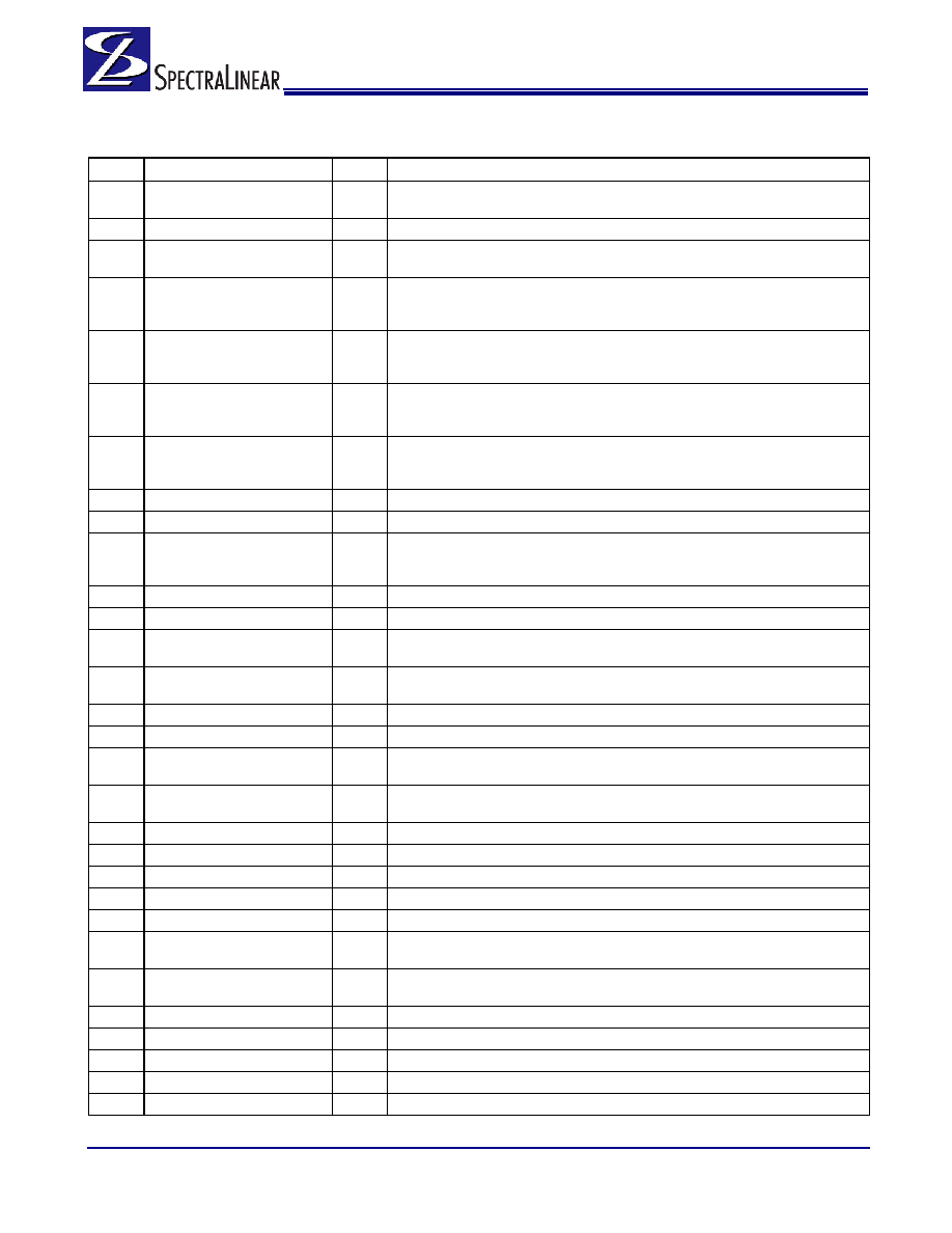
Pin Definitions
Pin No.
Name
Type
Description
1
PCI_0/OE#_0/2_A
I/O, SE 33 MHz clock/3.3V OE# Input mappable via I2C to control either SRC 0 or
SRC 2. Default PCI0
2
VDD_PCI
PWR
3.3V Power supply for PCI PLL.
3
PCI_1/OE#_1/4_A
I/O, SE 33 MHz clock/3.3V OE# Input mappable via I2C to control either SRC 1 or
SRC 4. Default PCI1.
4
PCI_2/TME
I/O, SE 3.3V tolerance input for overclocking enable pin 33 MHz clock.
Refer to DC Electrical Specifications table for Vil_FS and Vih_FS specifica-
tions.
5
PCI_3/CFG0
I/O, SE,
PD
3.3V tolerant input for CPU frequency selection/33 MHz clock.
Refer to DC Electrical Specifications table for Vil_PCI3/CFG0 and
Vih_PCI3/CFG0 specifications.
6
PCI_4/SRC5_SEL
I/O, SE 3.3V tolerant input to enable SRC5/33 MHz clock output.
(sampled on the CK_PWRGD assertion)
1 = SRC5, 0 = CPU_STOP#
7
PCIF_0/ITP_EN
I/O, SE 3.3V LVTTL input to enable SRC8 or CPU2_ITP/33 MHz clock output.
(sampled on the CK_PWRGD assertion)
1 = CPU2_ITP, 0 = SRC8
8
VSS_PCI
GND
Ground for outputs.
9
VDD_48
PWR
3.3V Power supply for outputs and PLL.
10
USB_48/FSA
I/O
3.3V tolerant input for CPU frequency selection/fixed 48 MHz clock output.
Refer to DC Electrical Specifications table for Vil_FS and Vih_FS specifica-
tions.
11
VSS_48
GND
Ground for outputs.
12
VDD_IO
PWR
0.7V Power supply for outputs.
13
SRC0/DOT96T
O, DIF 100 MHz Differential serial reference clocks/Fixed 96 MHz clock output.
Selected via I2C default is SRC0.
14
SRC0#/DOT96#
O, DIF 100 MHz Differential serial reference clocks/Fixed 96 MHz clock output.
Selected via I2C default is SRC0.
15
VSS_IO
GND
Ground for PLL2.
16
VDD_PLL3
PWR
3.3V Power supply for PLL3
17
SRC1/LCD_100/SE1
O, DIF,
SE
100 MHz Differential serial reference clocks/100 MHz LCD video clock/SE1
clocks. Default SRC1
18
SRC1#/LCD_100#/SE2
O, DIF,
SE
100 MHz Differential serial reference clocks/100 MHz LCD video clock/SE2
clocks. Default SRC1
19
VSS_PLL3
GND
Ground for PLL3.
20
VDD_PLL3_IO
PWR
0.7V Power supply for PLL3 outputs.
21
SRC2/SATA
O, DIF 100 MHz Differential serial reference clocks.
22
SRC2#/SATA#
O, DIF 100 MHz Differential serial reference clocks.
23
VSS_SRC
GND
Ground for outputs.
24
SRC3/OE#_0/2_B
I/O,
Dif
100-MHz Differential serial reference clocks / 3.3V OE#_0/2_B, input,
mappable via I2C to control either SRC 0 or SRC 2. Default SRC3
25
SRC3#OE#_1/4_B
I/O,
Dif
100-MHz Differential serial reference clocks / 3.3V OE#_1/4_B input,
mappable via I2C to control either SRC 1 or SRC 4. Default SRC3
26
VDD_SRC_IO
PWR
0.7V power supply for SRC outputs.
27
SRC4
O, DIF 100 MHz Differential serial reference clocks.
28
SRC4#
O, DIF 100 MHz Differential serial reference clocks.
29
VSS_SRC
GND
Ground for outputs.
30
SRC9
O, DIF 100 MHz Differential serial reference clocks.
相關(guān)PDF資料 |
PDF描述 |
|---|---|
| SPL505YC264BT | 400 MHz, PROC SPECIFIC CLOCK GENERATOR, PDSO64 |
| SPW08F0D | SINGLE COLOR LED, PURE WHITE, 3.5 mm |
| SSC-SFT825N-S | TRIPLE COLOR LED, RED/GREEN/BLUE, 2.4 mm |
| SSI32C452-CP | 20 Mbps, ST506; ST412; ST412HP; SA100 COMPATIBLE, FIXED DISK CONTROLLER, PDIP40 |
| SSO-CLD-JK2-1-I2 | SINGLE COLOR LED, ORANGE, 1.6 mm |
相關(guān)代理商/技術(shù)參數(shù) |
參數(shù)描述 |
|---|---|
| SPL505YC264BTT | 功能描述:時(shí)鐘發(fā)生器及支持產(chǎn)品 CK505 v0.85 RoHS:否 制造商:Silicon Labs 類型:Clock Generators 最大輸入頻率:14.318 MHz 最大輸出頻率:166 MHz 輸出端數(shù)量:16 占空比 - 最大:55 % 工作電源電壓:3.3 V 工作電源電流:1 mA 最大工作溫度:+ 85 C 安裝風(fēng)格:SMD/SMT 封裝 / 箱體:QFN-56 |
| SPL5100PT | 制造商:CHENMKO 制造商全稱:Chenmko Enterprise Co. Ltd. 功能描述:SCHOTTKY BARRIER RECTIFIER |
| SPL520LLPT | 制造商:CHENMKO 制造商全稱:Chenmko Enterprise Co. Ltd. 功能描述:SCHOTTKY BARRIER RECTIFIER |
| SPL53-1024 | 制造商:Power-One 功能描述: |
| SPL53-4000 | 制造商:Power-One 功能描述: |
發(fā)布緊急采購,3分鐘左右您將得到回復(fù)。