- 您現(xiàn)在的位置:買賣IC網(wǎng) > PDF目錄385856 > SP9842KS 8-Bit Octal, 2-Quadrant Multiplying, BiCMOS DAC PDF資料下載
參數(shù)資料
| 型號: | SP9842KS |
| 英文描述: | 8-Bit Octal, 2-Quadrant Multiplying, BiCMOS DAC |
| 中文描述: | 8位八路,2象限乘法,BiCMOS工藝援 |
| 文件頁數(shù): | 16/32頁 |
| 文件大小: | 745K |
| 代理商: | SP9842KS |
第1頁第2頁第3頁第4頁第5頁第6頁第7頁第8頁第9頁第10頁第11頁第12頁第13頁第14頁第15頁當(dāng)前第16頁第17頁第18頁第19頁第20頁第21頁第22頁第23頁第24頁第25頁第26頁第27頁第28頁第29頁第30頁第31頁第32頁
282
Pin 10 — V
OUT
G — DACG Voltage Output.
Pin 11 — V
OUT
H — DACH Voltage Output.
Pin 12 — V
IN
G/H — DACG and H Reference
Voltage Input.
Pin 13 — LOADH — Load DAC Register Strobe;
active high input that transfers the data bits from the
Serial Input Register into the decoded DAC Register.
Refer to Table 1.
Pin 14 — CLOCK — Serial Clock Input; positive–
edge triggered.
Pin 15 — SDO — Serial Data Output; active totem–
pole output.
Pin 16 — GND — Ground.
Pin 17 — SDI — Serial Data Input.
Pin 18 — V
DD
— Positive 5V Power Supply.
Pin 19 — V
IN
C/D — DACC and D Reference
Voltage Input.
Pin 20 — V
OUT
D — DACD Voltage Output.
FEATURES…
The
SP9841
and
SP9842
include eight separate op
amp–buffered eight–bit DACs. These can be used to
replace up to eight trimpots with eight low–imped-
ance programmable sources. The
SP9841
uses eight
separate multiplying reference inputs, while the
SP9842
provides four pair of multiplying inputs. All
of the reference inputs, in either case, are returned to
a common voltage reference low pin. The inherent 2X
gain from the two–quadrant multiplying reference
inputs to the outputs allows the use of AC or DC
multiplying reference inputs generated from a single,
low supply voltage.
Each DAC has its own data register which holds its
output state. These data registers are updated from an
internal serial-to-parallel shift register which is loaded
from a standard 3-wire serial input digital interface.
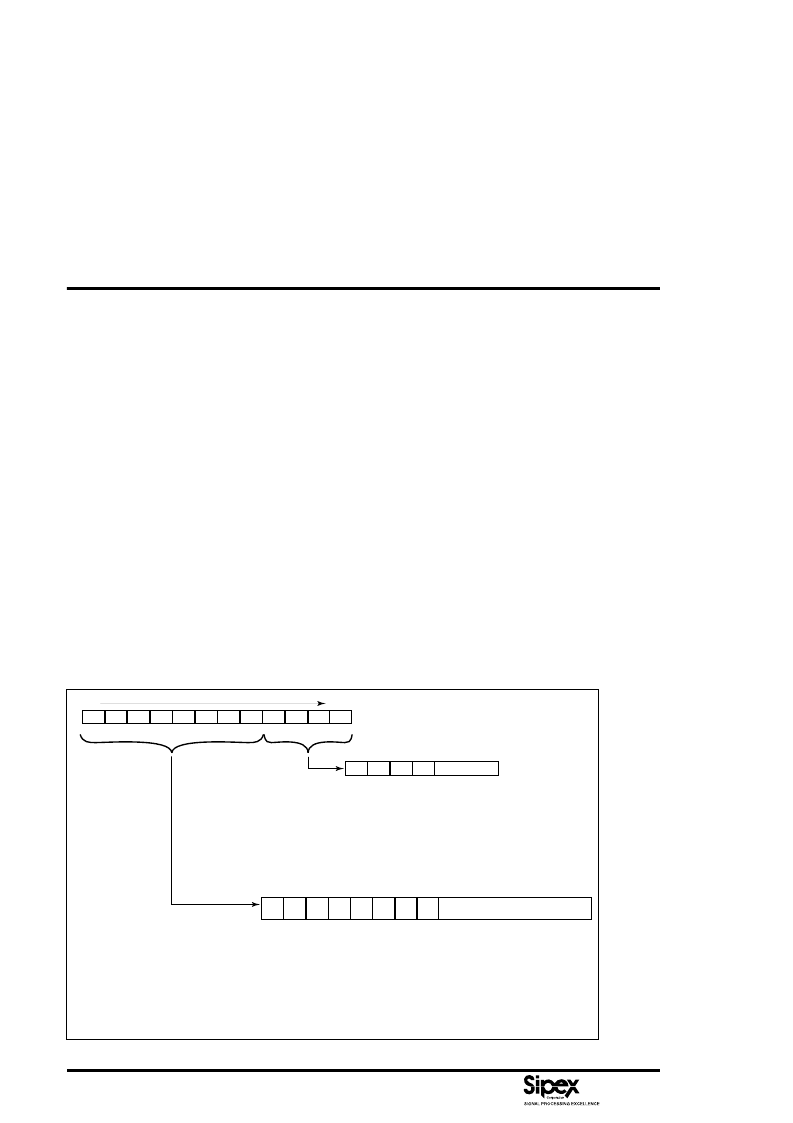
Twelve data bits make up the data word clocked into
the serial input register. This data word is decoded
such that the first 4 bits determine the address of the
DAC register to be loaded and the last 8 bits are the
data. A serial data output pin at the opposite end of the
serial register allows simple daisy-chaining in mul-
Table 1. Serial Input Decoded Truth Table
LAST
D
0
LSB
DATA
ADDRESS
D
1
D
2
D
3
D
4
D
5
D
6
D
7
MSB
D
7
D
6
D
5
D
4
D
3
D
2
D
1
D
0
DAC Output Voltage
V
OUT
= D/128 (V
IN
– V
REF
L) + V
REF
L
V
L
1/128 (V
IN
– V
REF
L) + V
REF
L
127/128 (V
– V
REF
L) + V
REF
L
V
(Preset Value)
129/128 (V
IN
– V
REF
L) + V
REF
L
254/128 (V
IN
– V
REF
L) + V
REF
L
255/128 (V
IN
– V
REF
L) + V
REF
L
A
0
LSB
A
1
A
2
A
3
MSB
A
3
0
0
0
0
0
0
0
0
1
1
A
2
0
0
0
0
1
1
1
1
0
0
.
.
1
A
1
0
0
1
1
0
0
1
1
0
0
.
.
1
A
0
0
1
0
1
0
1
0
1
0
1
.
.
1
DAC Updated
FIRST
.
.
1
0
0
0
1
1
1
1
0
0
1
0
0
1
1
0
0
1
0
0
1
1
0
0
1
0
0
1
1
0
0
1
0
0
.
.
.
1
1
0
0
1
0
0
1
1
0
0
1
0
0
1
1
0
1
1
0
1
0
1
No Operation
DACA
DACB
DACC
DACD
DACE
DACF
DACG
DACH
No Operation
.
.
No operation
.
.
.
.
.
.
.
.
.
相關(guān)PDF資料 |
PDF描述 |
|---|---|
| SPB04N60S5 | Cool MOS Power Transistor(MOS 型功率晶體管) |
| SPP04N60S5 | Cool MOS Power Transistor(MOS 型功率晶體管) |
| SPC-0605 | SMD POWER INDUCTORS |
| SPC-06502 | SMD POWER INDUCTORS |
| SPC-06502-100 | SMD POWER INDUCTORS |
相關(guān)代理商/技術(shù)參數(shù) |
參數(shù)描述 |
|---|---|
| SP9843 | 制造商:SIPEX 制造商全稱:Sipex Corporation 功能描述:8-Bit Octal, 4-Quadrant Multiplying, BiCMOS DAC |
| SP9843BS | 制造商:SIPEX 制造商全稱:Sipex Corporation 功能描述:8-Bit Octal, 4-Quadrant Multiplying, BiCMOS DAC |
| SP9843KS | 制造商:SIPEX 制造商全稱:Sipex Corporation 功能描述:8-Bit Octal, 4-Quadrant Multiplying, BiCMOS DAC |
| SP9908 | 制造商:BOTHHAND 制造商全稱:Bothhand USA, LP. 功能描述:39 Watts Switching Power Supply |
| SP9909 | 制造商:BOTHHAND 制造商全稱:Bothhand USA, LP. 功能描述:40~62 Watts Switching Power Supply |
發(fā)布緊急采購,3分鐘左右您將得到回復(fù)。