- 您現(xiàn)在的位置:買賣IC網(wǎng) > PDF目錄385795 > S29GL032M10BAIR63 (SPANSION LLC) MirrorBit Flash Family PDF資料下載
參數(shù)資料
| 型號(hào): | S29GL032M10BAIR63 |
| 廠商: | SPANSION LLC |
| 元件分類: | DRAM |
| 英文描述: | MirrorBit Flash Family |
| 中文描述: | 2M X 16 FLASH 3V PROM, 100 ns, PBGA48 |
| 封裝: | 8 X 6 MM, BGA-48 |
| 文件頁數(shù): | 29/159頁 |
| 文件大小: | 2217K |
| 代理商: | S29GL032M10BAIR63 |
第1頁第2頁第3頁第4頁第5頁第6頁第7頁第8頁第9頁第10頁第11頁第12頁第13頁第14頁第15頁第16頁第17頁第18頁第19頁第20頁第21頁第22頁第23頁第24頁第25頁第26頁第27頁第28頁當(dāng)前第29頁第30頁第31頁第32頁第33頁第34頁第35頁第36頁第37頁第38頁第39頁第40頁第41頁第42頁第43頁第44頁第45頁第46頁第47頁第48頁第49頁第50頁第51頁第52頁第53頁第54頁第55頁第56頁第57頁第58頁第59頁第60頁第61頁第62頁第63頁第64頁第65頁第66頁第67頁第68頁第69頁第70頁第71頁第72頁第73頁第74頁第75頁第76頁第77頁第78頁第79頁第80頁第81頁第82頁第83頁第84頁第85頁第86頁第87頁第88頁第89頁第90頁第91頁第92頁第93頁第94頁第95頁第96頁第97頁第98頁第99頁第100頁第101頁第102頁第103頁第104頁第105頁第106頁第107頁第108頁第109頁第110頁第111頁第112頁第113頁第114頁第115頁第116頁第117頁第118頁第119頁第120頁第121頁第122頁第123頁第124頁第125頁第126頁第127頁第128頁第129頁第130頁第131頁第132頁第133頁第134頁第135頁第136頁第137頁第138頁第139頁第140頁第141頁第142頁第143頁第144頁第145頁第146頁第147頁第148頁第149頁第150頁第151頁第152頁第153頁第154頁第155頁第156頁第157頁第158頁第159頁
Octorber 18, 2004 S29GLxxxM_00_B3
S29GLxxxM MirrorBit
TM
Flash Family
29
D a t a s h e e t
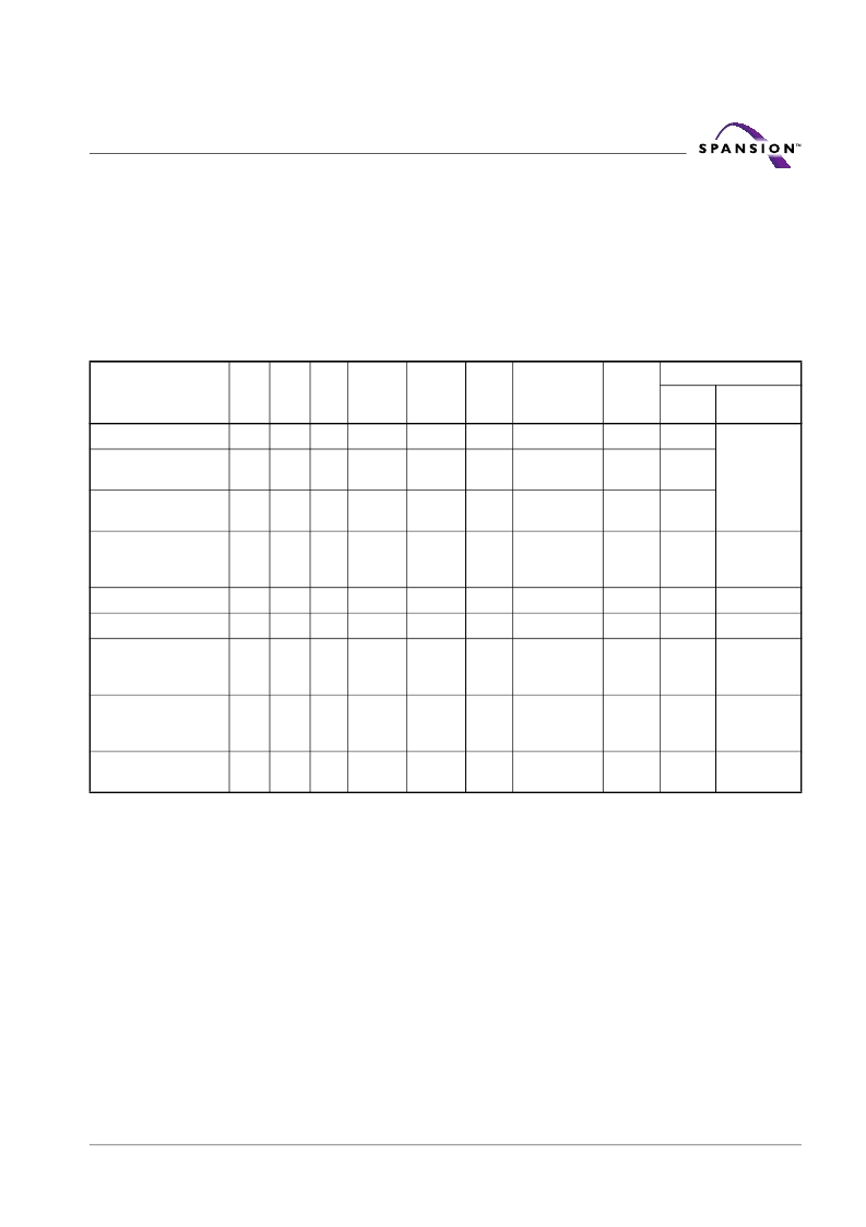
Device Bus Operations
This section describes the requirements and use of the device bus operations, which are initiated through the in-
ternal command register. The command register itself does not occupy any addressable memory location. The
register is a latch used to store the commands, along with the address and data information needed to execute
the command. The contents of the register serve as inputs to the internal state machine. The state machine out-
puts dictate the function of the device.
Table 5
lists the device bus operations, the inputs and control levels they
require, and the resulting output. The following subsections describe each of these operations in further detail.
Table 5. Device Bus Operations
Legend:
L = Logic Low = V
IL
, H = Logic High = V
IH
, V
ID
= 11.5–12.5
V, V
HH
= 11.5–12.5
V, X = Don’t Care, SA = Sector
Address, A
IN
= Address In, D
IN
= Data In, D
OUT
= Data Out
Notes:
1. Addresses are Amax:A0 in word mode; Amax:A-1 in byte mode. Sector addresses are Amax:A15 in both modes.
2. The sector protect and sector unprotect functions may also be implemented via programming equipment. See the
“Sector Group Protection and Unprotection” section.
3. If WP# = V
IL
, the first or last sector remains protected (for uniform sector devices), and the two outer boot sectors
are protected (for boot sector devices). If WP# = V
IH
, the first or last sector, or the two outer boot sectors are
protected or unprotected as determined by the method described in “Sector Group Protection and Unprotection”.
All sectors are unprotected when shipped from the factory (The SecSi Sector may be factory protected depending
on version ordered.)
4. D
IN
or D
OUT
as required by command sequence, data polling, or sector protect algorithm (see
Figure 2, on page 96
).
Operation
CE#
OE#
WE
#
RESET#
WP#
ACC
Addresses
(Note 1)
DQ0–
DQ7
DQ8–DQ15
BYTE#
= V
IH
BYTE#
= V
IL
Read
L
L
H
H
X
X
A
IN
D
OUT
D
OUT
DQ8–DQ14
= High-Z,
DQ15 = A-1
Write (Program/Erase)
L
H
L
H
(Note
3)
X
A
IN
(Note
4)
(Note
4)
Accelerated Program
L
H
L
H
(Note
3)
V
HH
A
IN
(Note
4)
(Note
4)
Standby
V
CC
±
0.3
V
X
X
V
CC
±
0.3 V
X
H
X
High-Z
High-Z
High-Z
Output Disable
L
H
H
H
X
X
X
High-Z
High-Z
High-Z
Reset
X
X
X
L
X
X
X
High-Z
High-Z
High-Z
Sector Group Protect
(Note 2)
L
H
L
V
ID
H
X
SA, A6 =L,
A3=L, A2=L,
A1=H, A0=L
(Note
4)
X
X
Sector Group
Unprotect
(Note 2)
L
H
L
V
ID
H
X
SA, A6=H,
A3=L, A2=L,
A1=H, A0=L
(Note
4)
X
X
Temporary Sector
Group Unprotect
X
X
X
V
ID
H
X
A
IN
(Note
4)
(Note
4)
High-Z
相關(guān)PDF資料 |
PDF描述 |
|---|---|
| S29GL032M10BFIR50 | MirrorBit Flash Family |
| S29GL032M10FBCR50 | MirrorBit Flash Family |
| S29GL064N11FFIV20 | 64 Megabit, 32 Megabit 3.0-Volt only Page Mode Flash Memory Featuring 110 nm MirrorBit Process Technology |
| S29GL064N11BFIV22 | 64 Megabit, 32 Megabit 3.0-Volt only Page Mode Flash Memory Featuring 110 nm MirrorBit Process Technology |
| S29GL064N11BFIV60 | 64 Megabit, 32 Megabit 3.0-Volt only Page Mode Flash Memory Featuring 110 nm MirrorBit Process Technology |
相關(guān)代理商/技術(shù)參數(shù) |
參數(shù)描述 |
|---|---|
| S29GL032M10BBCR00 | 制造商:SPANSION 制造商全稱:SPANSION 功能描述:MirrorBit Flash Family |
| S29GL032M10BBCR02 | 制造商:SPANSION 制造商全稱:SPANSION 功能描述:MirrorBit Flash Family |
| S29GL032M10BBCR03 | 制造商:SPANSION 制造商全稱:SPANSION 功能描述:MirrorBit Flash Family |
| S29GL032M10BBCR10 | 制造商:SPANSION 制造商全稱:SPANSION 功能描述:MirrorBit Flash Family |
| S29GL032M10BBCR12 | 制造商:SPANSION 制造商全稱:SPANSION 功能描述:MirrorBit Flash Family |
發(fā)布緊急采購,3分鐘左右您將得到回復(fù)。