- 您現(xiàn)在的位置:買賣IC網(wǎng) > PDF目錄373330 > RTL8201L Layout guide PDF資料下載
參數(shù)資料
| 型號(hào): | RTL8201L |
| 英文描述: | Layout guide |
| 中文描述: | 布局指南 |
| 文件頁數(shù): | 1/7頁 |
| 文件大小: | 73K |
| 代理商: | RTL8201L |
8201layoutguide(V1.00)
2000-11-08
REALTEK
Chip design & System design
1
RTL8201 PCB Layout Guide
1. Introduction
Goal : (1) Make a Noise-free, power-stable, environment that suitable for RTL8201.
(2) Reduce the possibility of EMI, EMC and their influence to the chip.
(3) Simplify the task of routing signal trace, so as to make a better circuit for
RTL8201.
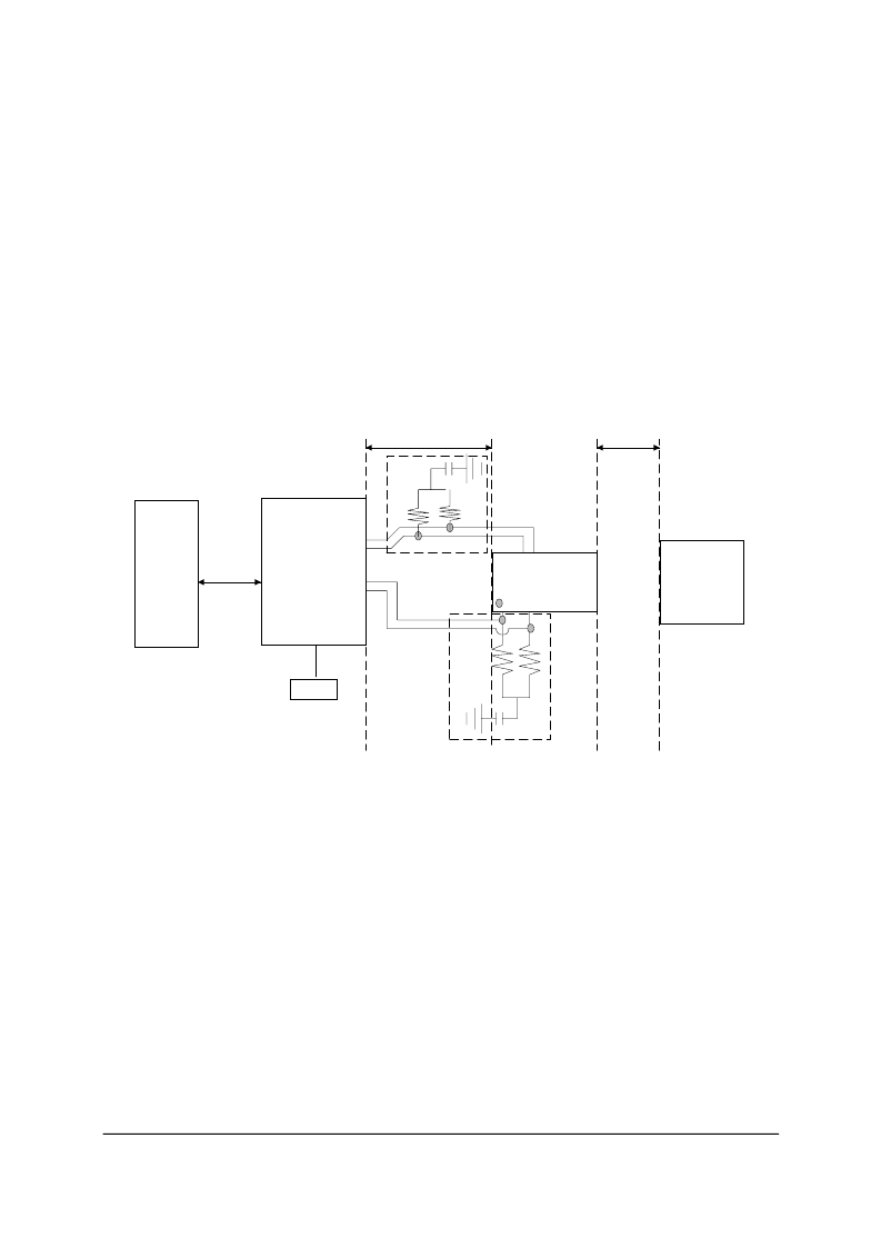
2. Placement
Ideally placement: as fellow
!
Block A should place as close to RTL8201 as possible. Block B may be placed
close to Mag. (Since when Tx, RTL8201 will sink current from Block A. When Rx,
RTL8201 will take differential volt signal from Block B.
!
The distance between RJ-45 to Mag. (L1) should be as short as possible.
!
RTset of RTL8201 pin 28 should placed as close to RTL8201 as possible and if
possible, it should be placed away from TX+/-,RX+/-, and clock signals
.
!
Crystal should not be placed near I/O ports and board edges and other high-freq.
devices or traces (such as Tx , Rx and Power signals) or magnetic field device (such
as magnetic).
!
The outer shield of Crystal need well grounding to avoid EMC/EMI to induce extra
noise, the retaining straps of the Crystal need well grounding, so as the case of
Crystal.
!
The magnetic device or devices with magnetic fields should be separated and
MII
Interface
Mag
RJ-45
L1
L2
A
B
OSC
RTL
8201
Tx
±
Rx
±
MAC
相關(guān)PDF資料 |
PDF描述 |
|---|---|
| RTL8204 | Layout reference |
| RTL8305SB | RTL8305SB |
| RTL8316 | Specifications |
| RTL8801 | Specifications |
| RTM5070 | IR LEUCHTELEMENT ZUR FRONTPLATTENMONTAGE |
相關(guān)代理商/技術(shù)參數(shù) |
參數(shù)描述 |
|---|---|
| RTL8201電路圖 | 制造商:未知廠家 制造商全稱:未知廠家 功能描述:RTL8201電路圖,RTL8201CP |
| RTL8204 | 制造商:未知廠家 制造商全稱:未知廠家 功能描述:Layout reference |
| RTL8208 | 制造商:未知廠家 制造商全稱:未知廠家 功能描述:REALTEK SINGLE CHIP OCTAL 10/100 MBPS FAST ETHERNET TRANSCEIVER |
| RTL8208C-GR | 制造商:Realtek Semiconductor 功能描述: |
| RTL8208電路圖-1 | 制造商:未知廠家 制造商全稱:未知廠家 功能描述:RTL8208電路圖-1,RTL8204 |
發(fā)布緊急采購(gòu),3分鐘左右您將得到回復(fù)。