- 您現(xiàn)在的位置:買賣IC網(wǎng) > PDF目錄372063 > RH80530NZ001256 Microprocessor PDF資料下載
參數(shù)資料
| 型號(hào): | RH80530NZ001256 |
| 英文描述: | Microprocessor |
| 中文描述: | 微處理器 |
| 文件頁數(shù): | 19/89頁 |
| 文件大小: | 1672K |
| 代理商: | RH80530NZ001256 |
第1頁第2頁第3頁第4頁第5頁第6頁第7頁第8頁第9頁第10頁第11頁第12頁第13頁第14頁第15頁第16頁第17頁第18頁當(dāng)前第19頁第20頁第21頁第22頁第23頁第24頁第25頁第26頁第27頁第28頁第29頁第30頁第31頁第32頁第33頁第34頁第35頁第36頁第37頁第38頁第39頁第40頁第41頁第42頁第43頁第44頁第45頁第46頁第47頁第48頁第49頁第50頁第51頁第52頁第53頁第54頁第55頁第56頁第57頁第58頁第59頁第60頁第61頁第62頁第63頁第64頁第65頁第66頁第67頁第68頁第69頁第70頁第71頁第72頁第73頁第74頁第75頁第76頁第77頁第78頁第79頁第80頁第81頁第82頁第83頁第84頁第85頁第86頁第87頁第88頁第89頁
Mobile Intel
Pentium
III Processor-M Datasheet
298340-002
Datasheet
19
3.
Electrical Specifications
3.1
Processor System Signals
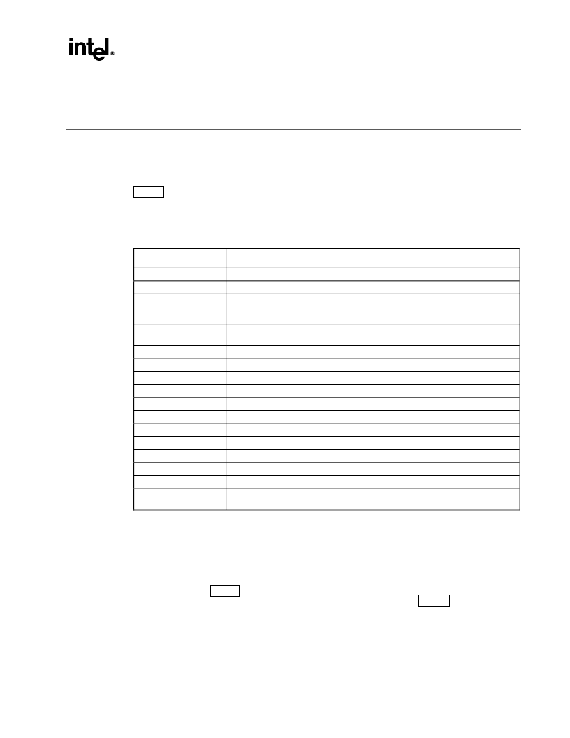
Table 5
lists the processor system signals by type. All AGTL signals are synchronous with the BCLK
and BCLK# signals. All TAP signals are synchronous with the TCK signal except TRST#. All CMOS
input signals can be applied asynchronously.
Table 5. System Signal Groups
Group Name
Signals
AGTL Input
BPRI#, DEFER#, RESET#, RSP#
AGTL Output
PRDY#
AGTL I/O
A[35:3]#, ADS#, AERR#, AP[1:0]#, BERR#, BINIT#, BNR#, BP[3:2]#, BPM[1:0]#,
BREQ0#, D[63:0]#, DBSY#, DEP[7:0]#, DRDY#, HIT#, HITM#, LOCK#, REQ[4:0]#,
RP#, RS[2:0]#, TRDY#
1.5V CMOS Input
A20M#, DPSLP#, FLUSH#, IGNNE#, INIT#, LINT0/INTR, LINT1/NMI, PREQ#, SMI#,
STPCLK#
1.8V CMOS Input
PWRGOOD
1.5V Open Drain Output
FERR#, IERR#
3.3V Open Drain Output
BSEL[1:0], VID[4:0]
1.25V input
GHI#, VTTPWRGD
Clock
BCLK, BCLK# (Differential Mode)
2.5V Clock Input
BCLK (Single Ended Mode)
APIC Clock
PICCLK
APIC I/O
PICD[1:0]
Thermal Diode
THERMDC, THERMDA
TAP Input
TCK, TDI, TMS, TRST#
TAP Output
TDO
Power/Other
CLKREF, CMOSREF, EDGECTRLP, NC, NCTRL, PLL1, PLL2, RTTIMPEDP, V
CC
,
V
CCT
, V
REF
, V
SS,
NOTES:
1. V
is the power supply for the core logic.
2. PLL1 and PLL2 are power/ground for the PLL analog section. See section 3.2.2 for details.
3. V
CCT
is the power supply for the system bus buffers.
4. V
REF
is the voltage reference for the AGTL input buffers.
5. V
SS
is system ground.
The APIC data and TAP outputs are Open-drain and should be pulled up to 1.5V using resistors with
the values shown in Table 6. If Open-drain drivers are used for input signals, then they should also be
pulled up to the appropriate voltage using resistors with the values shown in Table 6.
相關(guān)PDF資料 |
PDF描述 |
|---|---|
| RH80530NZ004256 | MICROPROCESSOR|32-BIT|CMOS|PGA|478PIN|CERAMIC |
| RH80530NZ006256 | MICROPROCESSOR|32-BIT|CMOS|PGA|478PIN|CERAMIC |
| RH80530NZ009256 | MICROPROCESSOR|32-BIT|CMOS|PGA|478PIN|CERAMIC |
| RH80530WZ014256 | Microprocessor |
| RJ80530GZ009512 | Microprocessor |
相關(guān)代理商/技術(shù)參數(shù) |
參數(shù)描述 |
|---|---|
| RH80530NZ001256S L6AB | 制造商:Intel 功能描述:MPU Celeron? Processor 64-Bit 0.13um 1GHz 478-Pin uFCPGA |
| RH80530NZ004256 | 制造商:未知廠家 制造商全稱:未知廠家 功能描述:MICROPROCESSOR|32-BIT|CMOS|PGA|478PIN|CERAMIC |
| RH80530NZ006256 | 制造商:未知廠家 制造商全稱:未知廠家 功能描述:MICROPROCESSOR|32-BIT|CMOS|PGA|478PIN|CERAMIC |
| RH80530NZ009256 | 制造商:未知廠家 制造商全稱:未知廠家 功能描述:MICROPROCESSOR|32-BIT|CMOS|PGA|478PIN|CERAMIC |
| RH80530NZ012256 | 制造商:Rochester Electronics LLC 功能描述:- Bulk |
發(fā)布緊急采購(gòu),3分鐘左右您將得到回復(fù)。