- 您現(xiàn)在的位置:買賣IC網(wǎng) > PDF目錄374589 > RFP4N40 (HARRIS SEMICONDUCTOR) 4A, 350V and 400V, 2.000 Ohm, N-Channel Power MOSFETs PDF資料下載
參數(shù)資料
| 型號(hào): | RFP4N40 |
| 廠商: | HARRIS SEMICONDUCTOR |
| 元件分類: | JFETs |
| 英文描述: | 4A, 350V and 400V, 2.000 Ohm, N-Channel Power MOSFETs |
| 中文描述: | 4 A, 400 V, 2 ohm, N-CHANNEL, Si, POWER, MOSFET, TO-204AA |
| 文件頁數(shù): | 2/4頁 |
| 文件大小: | 38K |
| 代理商: | RFP4N40 |
2
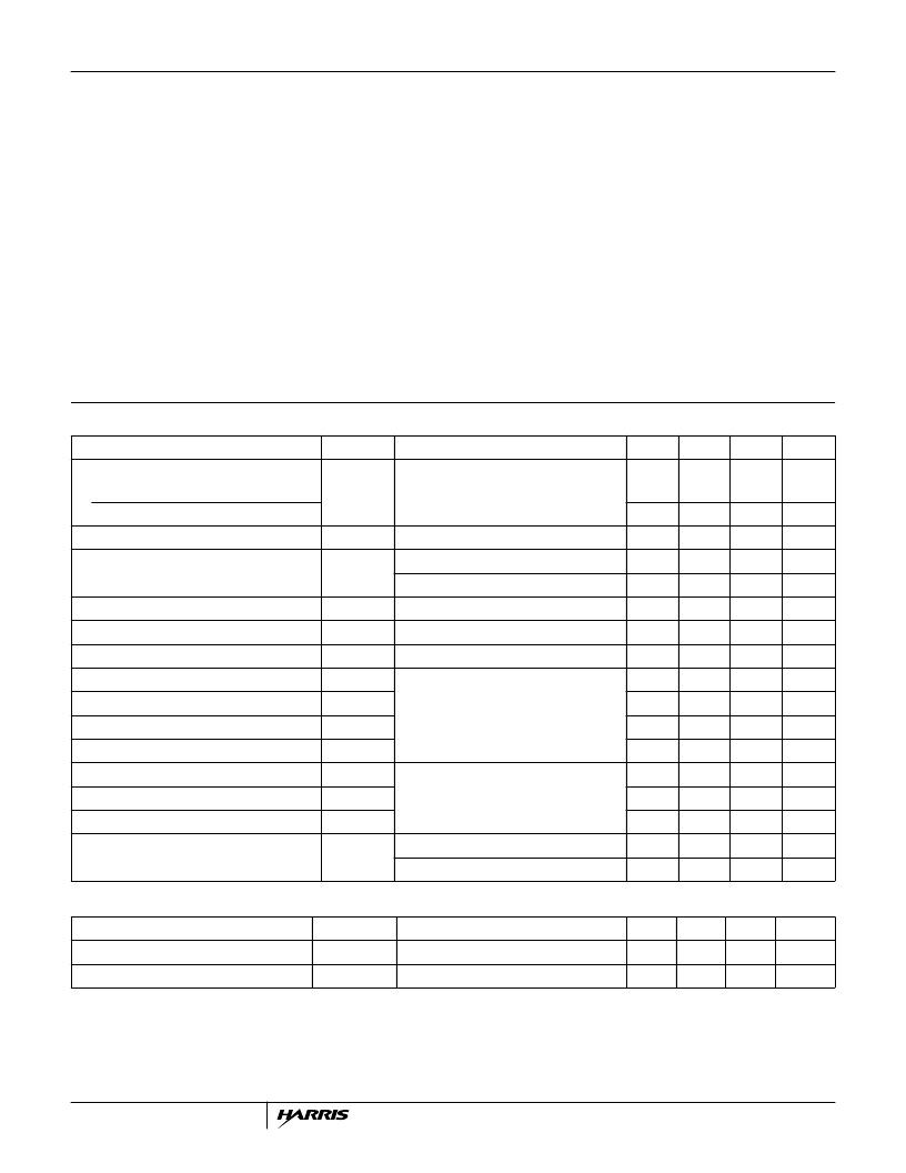
Absolute Maximum Ratings
T
C
= 25
o
C Unless Otherwise Specified
RFM4N35
350
350
4
8
±
20
75
0.6
-55 to 150
RFM4N40
400
400
4
8
±
20
75
0.6
-55 to 150
RFP4N35
350
350
4
8
±
20
60
0.48
-55 to 150
RFP4N40
400
400
4
8
±
20
60
0.48
-55 to 150
UNITS
V
V
A
A
V
W
W/
o
C
o
C
Drain to Source Voltage (Note 1). . . . . . . . . . . . . . . . . . . . . . . . . . .V
DS
Drain to Gate Voltage (R
GS
= 1M
)
(Note 1) . . . . . . . . . . . . . . . V
DGR
Continuous Drain Current . . . . . . . . . . . . . . . . . . . . . . . . . . . . . . . . . .I
D
Pulsed Drain Current (Note 3) . . . . . . . . . . . . . . . . . . . . . . . . . . . . . I
DM
Gate to Source Voltage . . . . . . . . . . . . . . . . . . . . . . . . . . . . . . . . . .V
GS
Maximum Power Dissipation . . . . . . . . . . . . . . . . . . . . . . . . . . . . . . .P
D
Linear Derating Factor . . . . . . . . . . . . . . . . . . . . . . . . . . . . . . . . . . . .
Operating and Storage Temperature . . . . . . . . . . . . . . . . . . . .T
J
, T
STG
Maximum Temperature for Soldering
Leads at 0.063in (1.6mm) from Case for 10s. . . . . . . . . . . . . . . . . T
L
Package Body for 10s, See Techbrief 334 (for TO-220). . . . . . . .T
pkg
CAUTION: Stresses above those listed in “Absolute Maximum Ratings” may cause permanent damage to the device. This is a stress only rating and operation of the
device at these or any other conditions above those indicated in the operational sections of this specification is not implied.
300
260
300
260
300
260
300
260
o
C
o
C
NOTE:
1. T
J
= 25
o
C to 125
o
C.
Electrical Specifications
T
C
= 25
o
C, Unless Otherwise Specified
PARAMETER
SYMBOL
TEST CONDITIONS
MIN
TYP
MAX
UNITS
Drain to Source Breakdown Voltage
RFM4N40, RFP4N40
BV
DSS
I
D
= 250
μ
A, V
GS
= 0
400
-
-
V
RFM4N35, RFP4N35
350
-
-
V
Gate Threshold Voltage
V
GS(TH)
V
GS
= V
DS
, I
D
= 250
μ
A (Figure 8)
2
-
4
V
Zero-Gate Voltage Drain Current
I
DSS
V
DS
= Rated BV
DSS
V
DS
= 0.8 x Rated BV
DSS
, T
C
= 125
o
C
-
-
1
μ
A
-
-
25
μ
A
Gate to Source Leakage Current
I
GSS
V
GS
=
±
20V, V
DS
= 0
-
-
±
100
nA
Drain to Source On Resistance (Note 2)
r
DS(ON)
I
D
= 4A, V
GS
= 10V (Figures 6, 7)
-
-
2.000
Drain to Source On-Voltage (Note 2)
V
DS(ON)
I
D
= 4A, V
GS
= 10V
-
-
8
V
Turn-On Delay Time
t
D(ON)
V
DD
= 200V, I
D
= 2A, R
G
= 50
R
L
= 100
, V
GS
= 10V
(Figures 10, 11, 12)
-
12
45
ns
Rise Time
t
r
-
42
60
ns
Turn-Off Delay Time
t
D(OFF)
-
130
200
ns
Fall Time
t
f
-
62
100
ns
Input Capacitance
C
ISS
V
DS
= 25V,
V
GS
= 0V
f = 1MHz (Figure 9)
-
-
750
pF
Output Capacitance
C
OSS
-
-
150
pF
Reverse-Transfer Capacitance
C
RSS
-
-
100
pF
Thermal Resistance Junction to Case
R
θ
JC
RFM4N35, RFM4N40
-
-
1.67
o
C/W
RFP4N35, RFP4N40
-
-
2.083
o
C/W
Source to Drain Diode Specifications
PARAMETER
SYMBOL
TEST CONDITIONS
MIN
TYP
MAX
UNITS
Source to Drain Diode Voltage (Note 2)
V
SD
I
SD
= 2A
-
-
1.4
V
Reverse Recorvery Time
t
rr
I
SD
= 4A, dI
SD
/dt = 100A/
μ
s
-
800
-
ns
NOTES:
2. Pulse Test: Pulse Width
≤
300
μ
s, Duty Cycle
≤
2%.
3. Repetitive rating: pulse width limited by maximum junction temperature.
RFM4N35, RFM4N40, RFP4N35, RFP4N40
相關(guān)PDF資料 |
PDF描述 |
|---|---|
| RFM4N35 | 4A, 350V and 400V, 2.000 Ohm, N-Channel Power MOSFETs |
| RFM4N40 | 4A, 350V and 400V, 2.000 Ohm, N-Channel Power MOSFETs |
| RFP6N50 | 6A, 450V and 500V, 1.250 Ohm, N-Channel Power MOSFETs |
| RFP6N45 | 6A, 450V and 500V, 1.250 Ohm, N-Channel Power MOSFETs |
| RFM6N45 | 6A, 450V and 500V, 1.250 Ohm, N-Channel Power MOSFETs |
相關(guān)代理商/技術(shù)參數(shù) |
參數(shù)描述 |
|---|---|
| RFP50 | 制造商:Panasonic Industrial Company 功能描述:SUB ONLY RADIO |
| RF-P50 | 制造商:Panasonic Industrial Company 功能描述:SUB ONLY POCKET AM/FM RADIOPANASONIC |
| RFP-500-50N-D | 制造商:未知廠家 制造商全稱:未知廠家 功能描述:Cable & Coaxial Terminations |
| RFP-50-100RCG | 制造商:ANAREN 制造商全稱:Anaren Microwave 功能描述:Flanged Resistors |
| RFP-50-50RCG-S | 制造商:ANAREN 制造商全稱:Anaren Microwave 功能描述:Flanged Resistor 50 Watts, 50Ohms |
發(fā)布緊急采購,3分鐘左右您將得到回復(fù)。