- 您現(xiàn)在的位置:買賣IC網(wǎng) > PDF目錄373259 > REFERENCEMANUAL Reference Manual - ElanSC400 Register Set Reference Manual (Including Changes for the 蒷anSC410 Microcontroller) PDF資料下載
參數(shù)資料
| 型號: | REFERENCEMANUAL |
| 英文描述: | Reference Manual - ElanSC400 Register Set Reference Manual (Including Changes for the 蒷anSC410 Microcontroller) |
| 中文描述: | 參考手冊- ElanSC400寄存器組參考手冊(包括微控制器的蒷anSC410變化) |
| 文件頁數(shù): | 2/40頁 |
| 文件大?。?/td> | 405K |
| 代理商: | REFERENCEMANUAL |
第1頁當前第2頁第3頁第4頁第5頁第6頁第7頁第8頁第9頁第10頁第11頁第12頁第13頁第14頁第15頁第16頁第17頁第18頁第19頁第20頁第21頁第22頁第23頁第24頁第25頁第26頁第27頁第28頁第29頁第30頁第31頁第32頁第33頁第34頁第35頁第36頁第37頁第38頁第39頁第40頁
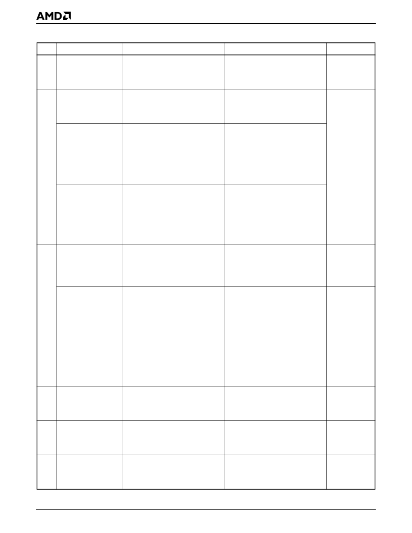
2
élanSC400 Microcontroller Register Set Reference Manual Amendment
A M E N D M E N T
2-49
PC/AT Keyboard
Mouse Interface Status
Register, Address
0064h; bit 5 description
When CSC index C0h[0] is set, this
bit is a PC/2 mouse-compatible
mouse output buffer full flay...
When CSC index C0h[0] is set, this
bit is a PS/2 mouse-compatible
mouse output buffer full flag...
Two corrections:
“PS/2 mouse”
and “flag.”
2-52
RTC/CMOS RAM
Index Register,
Address 0070h;
diagram (bit 7 column)
Reserved
–
NMI_GATE
0
W
The NMI_GATE
function has
not
moved to CSC
index 9Dh[2] in
the élanSC400
or élanSC410
microcontrollers.
RTC/CMOS RAM
Index Register,
Address 0070h; bit 7
description
7 Reserved
Reserved
During read/modify/
write operations,
software must
preserve this bit.
7 NMI_GATE
Master NMI Mask
1 = NMI events are
gated off from
reaching the core
0 = NMI events will
propagate to the CPU
core
RTC/CMOS RAM
Index Register,
Address 0070h;
Programming Notes
Programming Notes
Bit 7 of this register is the master NMI
gate control in a typical PC/AT
Compatible system. For various
reason, this bit has been made to
reside at CSC index 9Dh[2]...
(entire paragraph)
Programming Notes
2-92
Master Software
DRQ(n) Request
Register, Address
00D2h; default bit
values in diagram
0 0 0 0 0 0 0 0
x x x x x x x x
“x” = non-
deterministic.
Master Software
DRQ(n) Request
Register, Address
00D2h; bits 1–0
description
0 0 =
Mask/unmask DMA Channel
4 mask per the REQDMA bit
Mask/unmask DMA Channel
5 mask per the REQDMA bit
Mask/unmask DMA Channel
6 mask per the REQDMA bit
Mask/unmask DMA Channel
7 mask per the REQDMA bit
0 1 =
1 0 =
1 1 =
0 0 =
Set/Reset DMA Channel 4
internal DMA request per the
REQDMA bit
Set/Reset DMA Channel 5
internal DMA request per the
REQDMA bit
Set/Reset DMA Channel 6
internal DMA request per the
REQDMA bit
Set/Reset DMA Channel 7
internal DMA request per the
REQDMA bit
0 1 =
1 0 =
1 1 =
This field selects
the DMA
request channel
to assert or
deassert,
depending on
the state of bit 2.
2-93
Master DMA Mask
Register Channels 4–7,
Address 00D4h; default
bit values in diagram
0 0 0 0 0 0 0 0
x x x x x x x x
“x” = non-
deterministic.
2-94
Master DMA Mode
Register Channels 4–7,
Address 00D6h; default
bit values in diagram
0 0 0 0 0 0 0 0
x x x x x x x x
“x” = non-
deterministic.
2-95
Master DMA Clear Byte
Pointer Register,
Address 00D8h; default
bit values in diagram
0 0 0 0 0 0 0 0
x x x x x x x x
“x” = non-
deterministic.
Table 1.
Corrections to the
élanSC400 Microcontroller Register Set Reference Manual
(Continued)
Page Item
Original Text
Change To
Comment
相關(guān)PDF資料 |
PDF描述 |
|---|---|
| REG103-25 | DMOS 500mA Low Dropout (LDO) Regulator |
| REG103-27 | DMOS 500mA Low Dropout (LDO) Regulator |
| REG103-3 | DMOS 500mA Low Dropout (LDO) Regulator |
| REG103-33 | DMOS 500mA Low Dropout (LDO) Regulator |
| REG103-5 | DMOS 500mA Low Dropout (LDO) Regulator |
相關(guān)代理商/技術(shù)參數(shù) |
參數(shù)描述 |
|---|---|
| REF-H100 | 制造商:PEPPERL+FUCHS 功能描述:PHOTO ACCESSORY - REFLECTOR |
| REF-H100-2R | 制造商:PEPPERL+FUCHS 功能描述:Photoelectric (Automation) |
| REF-H180 | 制造商:PEPPERL+FUCHS 功能描述:Reflector, Photoelectric, Rectangular, 180mm x 40mm x 7.4mm, 2 Mounting Holes |
| REF-H23 | 制造商:PEPPERL+FUCHS 功能描述:Reflector, rectangular, 14 mm x 19 mm |
| REF-H32 | 制造商:PEPPERL+FUCHS 功能描述:Reflector, Hexagonal, 55mm x 25mm Size, w/Mounting Holes 制造商:PEPPERL+FUCHS 功能描述:SENSOR REFLECTOR 制造商:PEPPERL+FUCHS 功能描述:SENSOR REFLECTOR; Reflector Type:Corner Cube; Accessory Type:Reflector; For Use With:All Photoelectric Sensors; Size:2.2 x 1 x 0.37 in; Temperature Max:65C; Type:Side Mounting Holes ;RoHS Compliant: Yes |
發(fā)布緊急采購,3分鐘左右您將得到回復。