- 您現(xiàn)在的位置:買(mǎi)賣(mài)IC網(wǎng) > PDF目錄16874 > PCM18XT0 (Microchip Technology)MODULE PROC PIC18F4685 PDF資料下載
參數(shù)資料
| 型號(hào): | PCM18XT0 |
| 廠商: | Microchip Technology |
| 文件頁(yè)數(shù): | 179/183頁(yè) |
| 文件大小: | 0K |
| 描述: | MODULE PROC PIC18F4685 |
| 標(biāo)準(zhǔn)包裝: | 1 |
| 附件類型: | 處理器模塊 |
| 適用于相關(guān)產(chǎn)品: | ICE2000 |
| 產(chǎn)品目錄頁(yè)面: | 658 (CN2011-ZH PDF) |
| 配用: | ICE2000-ND - EMULATOR MPLAB-ICE 2000 POD |
| 相關(guān)產(chǎn)品: | DVA18XP400-ND - DEVICE ADAPTER 18F4220 PDIP 40LD DVA18XP280-ND - DEVICE ADAPTER 18F2220 PDIP 28LD DVA18PQ440-ND - DEVICE ADAPTER 18F4220 TQFP 44LD |
第1頁(yè)第2頁(yè)第3頁(yè)第4頁(yè)第5頁(yè)第6頁(yè)第7頁(yè)第8頁(yè)第9頁(yè)第10頁(yè)第11頁(yè)第12頁(yè)第13頁(yè)第14頁(yè)第15頁(yè)第16頁(yè)第17頁(yè)第18頁(yè)第19頁(yè)第20頁(yè)第21頁(yè)第22頁(yè)第23頁(yè)第24頁(yè)第25頁(yè)第26頁(yè)第27頁(yè)第28頁(yè)第29頁(yè)第30頁(yè)第31頁(yè)第32頁(yè)第33頁(yè)第34頁(yè)第35頁(yè)第36頁(yè)第37頁(yè)第38頁(yè)第39頁(yè)第40頁(yè)第41頁(yè)第42頁(yè)第43頁(yè)第44頁(yè)第45頁(yè)第46頁(yè)第47頁(yè)第48頁(yè)第49頁(yè)第50頁(yè)第51頁(yè)第52頁(yè)第53頁(yè)第54頁(yè)第55頁(yè)第56頁(yè)第57頁(yè)第58頁(yè)第59頁(yè)第60頁(yè)第61頁(yè)第62頁(yè)第63頁(yè)第64頁(yè)第65頁(yè)第66頁(yè)第67頁(yè)第68頁(yè)第69頁(yè)第70頁(yè)第71頁(yè)第72頁(yè)第73頁(yè)第74頁(yè)第75頁(yè)第76頁(yè)第77頁(yè)第78頁(yè)第79頁(yè)第80頁(yè)第81頁(yè)第82頁(yè)第83頁(yè)第84頁(yè)第85頁(yè)第86頁(yè)第87頁(yè)第88頁(yè)第89頁(yè)第90頁(yè)第91頁(yè)第92頁(yè)第93頁(yè)第94頁(yè)第95頁(yè)第96頁(yè)第97頁(yè)第98頁(yè)第99頁(yè)第100頁(yè)第101頁(yè)第102頁(yè)第103頁(yè)第104頁(yè)第105頁(yè)第106頁(yè)第107頁(yè)第108頁(yè)第109頁(yè)第110頁(yè)第111頁(yè)第112頁(yè)第113頁(yè)第114頁(yè)第115頁(yè)第116頁(yè)第117頁(yè)第118頁(yè)第119頁(yè)第120頁(yè)第121頁(yè)第122頁(yè)第123頁(yè)第124頁(yè)第125頁(yè)第126頁(yè)第127頁(yè)第128頁(yè)第129頁(yè)第130頁(yè)第131頁(yè)第132頁(yè)第133頁(yè)第134頁(yè)第135頁(yè)第136頁(yè)第137頁(yè)第138頁(yè)第139頁(yè)第140頁(yè)第141頁(yè)第142頁(yè)第143頁(yè)第144頁(yè)第145頁(yè)第146頁(yè)第147頁(yè)第148頁(yè)第149頁(yè)第150頁(yè)第151頁(yè)第152頁(yè)第153頁(yè)第154頁(yè)第155頁(yè)第156頁(yè)第157頁(yè)第158頁(yè)第159頁(yè)第160頁(yè)第161頁(yè)第162頁(yè)第163頁(yè)第164頁(yè)第165頁(yè)第166頁(yè)第167頁(yè)第168頁(yè)第169頁(yè)第170頁(yè)第171頁(yè)第172頁(yè)第173頁(yè)第174頁(yè)第175頁(yè)第176頁(yè)第177頁(yè)第178頁(yè)當(dāng)前第179頁(yè)第180頁(yè)第181頁(yè)第182頁(yè)第183頁(yè)
2011 Microchip Technology Inc.
DS39931D-page 95
PIC18F46J50 FAMILY
RPINR3
—
Input Function INT3 to Input Pin Mapping Bits
---1 1111
RPINR2
—
Input Function INT2 to Input Pin Mapping Bits
---1 1111
RPINR1
—
Input Function INT1 to Input Pin Mapping Bits
---1 1111
RPOR24(5)
—
Remappable Pin RP24 Output Signal Select Bits
---0 0000
RPOR23(5)
—
Remappable Pin RP23 Output Signal Select Bits
---0 0000
RPOR22(5)
—
Remappable Pin RP22 Output Signal Select Bits
---0 0000
RPOR21(5)
—
Remappable Pin RP21 Output Signal Select Bits
---0 0000
RPOR20(5)
—
Remappable Pin RP20 Output Signal Select Bits
---0 0000
RPOR19(5)
—
Remappable Pin RP19 Output Signal Select Bits
---0 0000
RPOR18
—
Remappable Pin RP18 Output Signal Select Bits
---0 0000
RPOR17
—
Remappable Pin RP17 Output Signal Select Bits
---0 0000
RPOR13
—
Remappable Pin RP13 Output Signal Select Bits
---0 0000
RPOR12
—
Remappable Pin RP12 Output Signal Select Bits
---0 0000
RPOR11
—
Remappable Pin RP11 Output Signal Select Bits
---0 0000
RPOR10
—
Remappable Pin RP10 Output Signal Select Bits
---0 0000
RPOR9
—
Remappable Pin RP9 Output Signal Select Bits
---0 0000
RPOR8
—
Remappable Pin RP8 Output Signal Select Bits
---0 0000
RPOR7
—
Remappable Pin RP7 Output Signal Select Bits
---0 0000
RPOR6
—
Remappable Pin RP6 Output Signal Select Bits
---0 0000
RPOR5
—
Remappable Pin RP5 Output Signal Select Bits
---0 0000
RPOR4
—
Remappable Pin RP4 Output Signal Select Bits
---0 0000
RPOR3
—
Remappable Pin RP3 Output Signal Select Bits
---0 0000
RPOR2
—
Remappable Pin RP2 Output Signal Select Bits
---0 0000
RPOR1
—
Remappable Pin RP1 Output Signal Select Bits
---0 0000
RPOR0
—
Remappable Pin RP0 Output Signal Select Bits
---0 0000
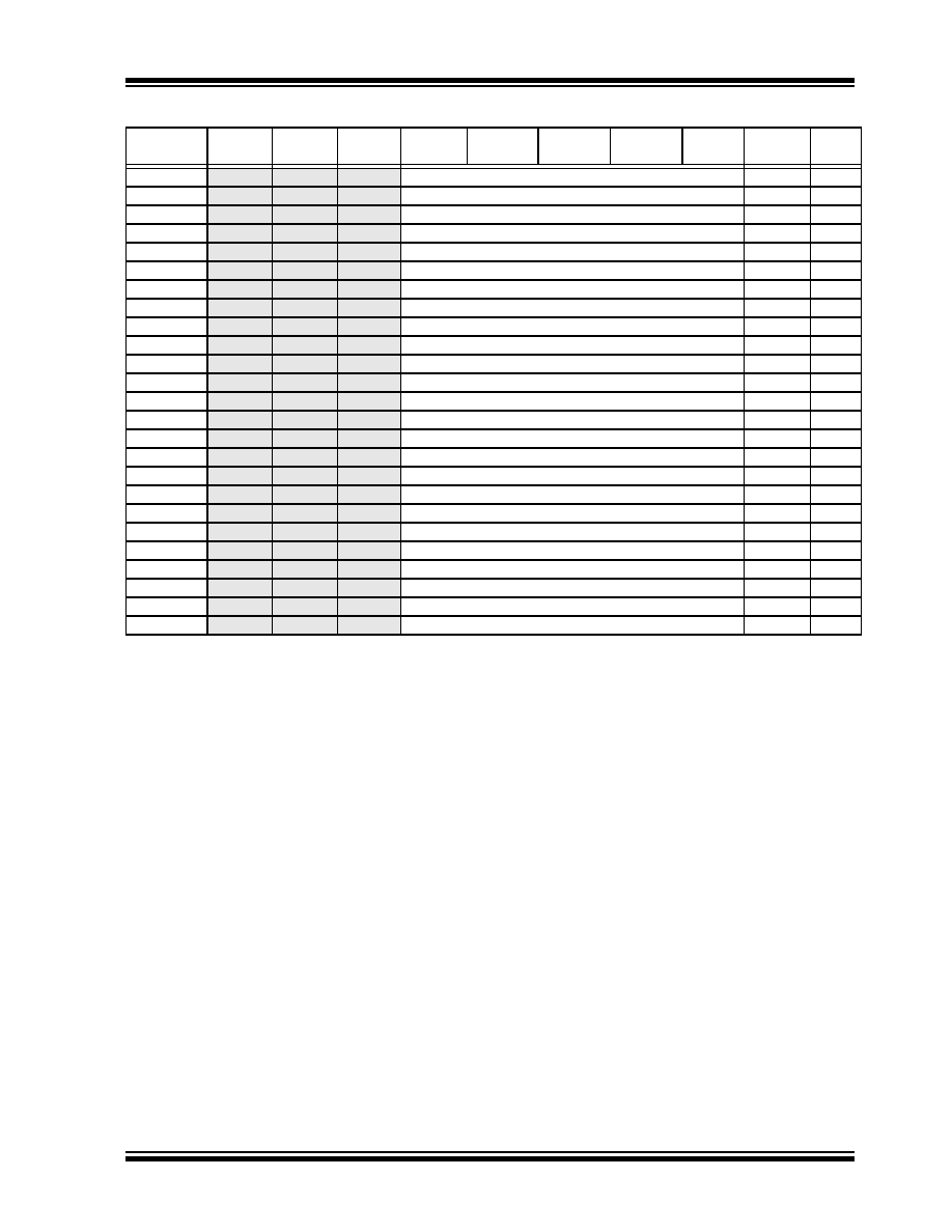
TABLE 6-4:
REGISTER FILE SUMMARY (PIC18F46J50 FAMILY) (CONTINUED)
File Name
Bit 7
Bit 6
Bit 5
Bit 4
Bit 3
Bit 2
Bit 1
Bit 0
Value on
POR, BOR
Details
on Page:
Legend:
x
= unknown, u = unchanged, - = unimplemented, q = value depends on condition, r = reserved. Bold indicates shared access SFRs.
Note
1:
Bit 21 of the PC is only available in Serial Programming (SP) modes.
2:
Reset value is ‘0’ when Two-Speed Start-up is enabled and ‘1’ if disabled.
3:
The SSPxMSK registers are only accessible when SSPxCON2<3:0> = 1001.
4:
Alternate names and definitions for these bits when the MSSP module is operating in I2C Slave mode. See Section 19.5.3.2 “Address
Masking Modes”
for details.
5:
These bits and/or registers are only available on 44-pin devices; otherwise, they are unimplemented and read as ‘0’. Reset values are
shown for 44-pin devices.
6:
The PMADDRH/PMDOUT1H and PMADDRL/PMDOUT1L register pairs share the same physical registers and addresses, but have
different functions determined by the module’s operating mode. See Section 11.1.2 “Data Registers” for more information.
7:
The TRISA6 and TRISA7 bits are only implemented when the pins are not configured for primary oscillator functions.
相關(guān)PDF資料 |
PDF描述 |
|---|---|
| MAX6220ASA-5.0+T | IC VREF SERIES PREC 5V 8-SOIC |
| RPP20-4824DW-F | CONV DC/DC 20W 18-75VIN +/-24VOU |
| GCC31DCSH-S288 | CONN EDGECARD 62POS .100 EXTEND |
| XRP2525ID-1-F | IC PWR SW USB 3.0 SINGLE NSOIC8 |
| PCM16XV0 | PROCESSOR MODULE FOR 16F8XXA |
相關(guān)代理商/技術(shù)參數(shù) |
參數(shù)描述 |
|---|---|
| PCM-19 | 功能描述:電線鑒定 1.5" VINYL CLOTH #19 RoHS:否 制造商:TE Connectivity / Q-Cees 產(chǎn)品:Labels and Signs 類型: 材料:Vinyl 顏色:Blue 寬度:0.625 in 長(zhǎng)度:1 in |
| PCM-1-9 | 制造商:Panduit Corp 功能描述:Cable Markers Vinyl Cloth White 制造商:Panduit Corp 功能描述:CBL ACC WIRE MARKER CARD VINYL CLOTH BLK/WHITE - Labels that come on sheets or rolls |
| PCM-190 | 功能描述:電線鑒定 Pre-Printed WM Card, Vinyl Cloth, .22" W RoHS:否 制造商:TE Connectivity / Q-Cees 產(chǎn)品:Labels and Signs 類型: 材料:Vinyl 顏色:Blue 寬度:0.625 in 長(zhǎng)度:1 in |
| PCM-1900-06 | 制造商:PREMIER FARNELL 功能描述:6 NULL MODEM DB25 M/F CABLE |
| PCM-1900-1924 | 制造商:Panduit Corp 功能描述: |
發(fā)布緊急采購(gòu),3分鐘左右您將得到回復(fù)。