- 您現(xiàn)在的位置:買賣IC網(wǎng) > PDF目錄383731 > OZ6933 (Electronic Theatre Controls, Inc.) ACPI CardBus Controller PDF資料下載
參數(shù)資料
| 型號(hào): | OZ6933 |
| 廠商: | Electronic Theatre Controls, Inc. |
| 英文描述: | ACPI CardBus Controller |
| 中文描述: | ACPI的CardBus控制器 |
| 文件頁(yè)數(shù): | 13/15頁(yè) |
| 文件大小: | 126K |
| 代理商: | OZ6933 |
第1頁(yè)第2頁(yè)第3頁(yè)第4頁(yè)第5頁(yè)第6頁(yè)第7頁(yè)第8頁(yè)第9頁(yè)第10頁(yè)第11頁(yè)第12頁(yè)當(dāng)前第13頁(yè)第14頁(yè)第15頁(yè)
OZ6933
OZ6933-SF-1.7
Page 13
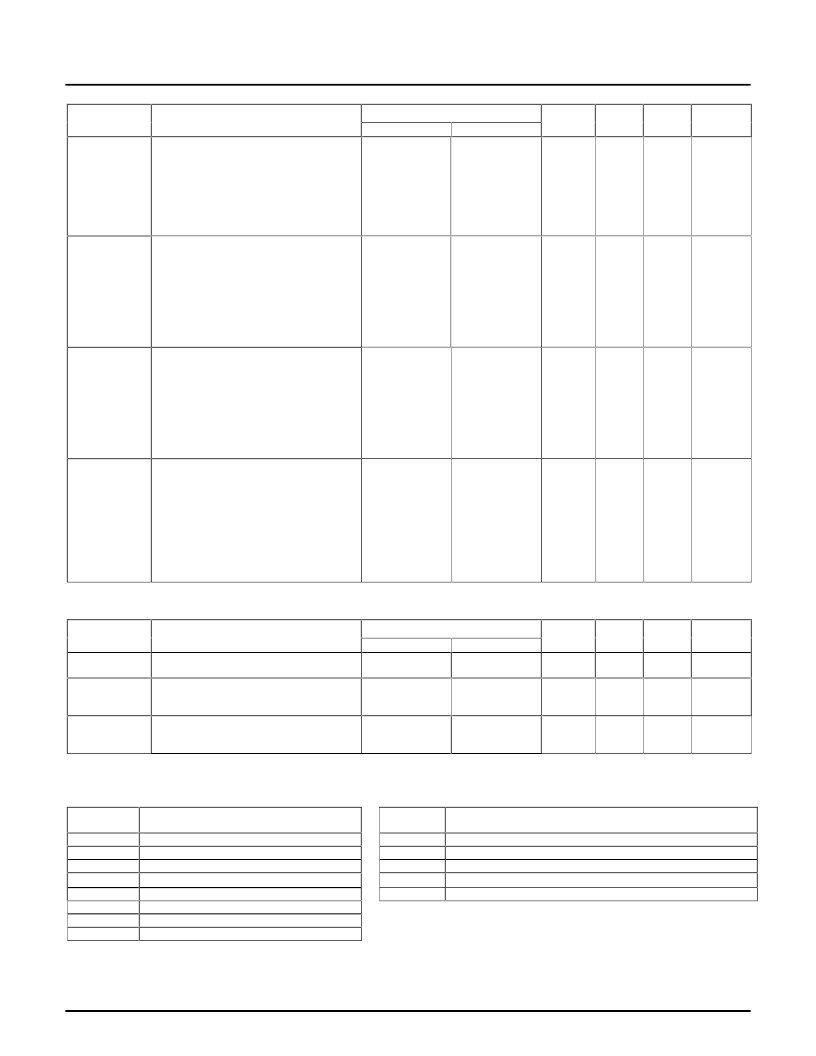
Pin Number
TQFP
87
Pin Name
Description
BGA
W12
Input
Type
Power
Rail
1
Drive
IRQ3/
A_VCC3#
A_VCC3#/IRQ3
: This active-LOW output
controls of the 3.3-volt supply to the
socket
’
s VCC pins. The active-LOW level
of this output is mutually exclusive with of
VCC_5#.
This mode active only in
SktPwr Parallel mode enabled.
This pin can be IRQ3 in parallel IRQ
mode.
VPP_VCC/IRQ9:
output controls the socket A VCC supply
to the socket
’
s VPP1 and VPP2 pins.
The active-HIGH level of this output is
mutually
exclusive
VPP_PGM.
This mode active only in
SktPwr Parallel mode enabled
This pin can be configured as IRQ9 in
parallel IRQ mode.
VPP_VCC/IRQ10:
output controls the socket B VCC supply
to the socket
’
s VPP1 and VPP2 pins.
The active-HIGH level of this output is
mutually
exclusive
VPP_PGM.
This mode active only in
SktPwr Parallel mode enabled.
This pin can be configured as IRQ10 in
parallel IRQ mode.
Global_Reset#:
This signal can be
connected to either PCI reset or ACPI
reset
depending
implementation. If the D3 cold state is
implemented, this signal should be
connected to the ACPI reset, otherwise,
connect to PCI reset.
This signal can reset the PME content
under the D3 cold state if AUX_VCC is
provided
N/A
TO
6mA
IRQ9/
A_VPP_VCC
This
active-HIGH
with
that
of
115
P19
N/A
TO
1
6mA
IRQ10/
B_VPP_VCC
This
active-HIGH
with
that
of
146
F19
N/A
TO
1
6mA
G_RST#
on
system
117
N18
TTL
I
1
-
Power, Ground, and Reserved Pins
Pin Number
TQFP
127
Pin Name
Description
BGA
L15
Input
Type
Power
Rail
-
Drive
AUX_VCC
This pin must be connected to the
system
’
s 3.3-volt supply.
This pin provides power to the core
circuitry of the OZ6933. It must be
connected to a 3.3 power supply.
All OZ6933 ground pins must be
connected to system ground.
N/A
PWR
-
CORE_VCC
180, 134, 79
B10, J18, R10
N/A
PWR
-
-
GND
14, 26, 28, 44,
57, 101, 129,
177
H3, K5, K5, P2,
W5, V15, K18,
E11
N/A
GND
-
-
Legend
I/O Type
Description
Power
Rail
1
2
3
4
5
Source of Output’s Power
I
Input Pin
Input pin with internal pull-up
Output
Open-drain
Tri-state output
Tri-state output with internal pull-up
Open-drain output with internal pull-up
Power pin
AUX_VCC: outputs powered from AUX_VCC
A_SLOT_VCC: outputs powered from the socket A
B_SLOT_VCC: outputs powered from the socket B
PCI_VCC: outputs powered from PCI bus power supply
CORE_VCC: outputs powered from the CORE_VCC
I-PU
O
OD
TO
TO-PU
OD-PU
PW
相關(guān)PDF資料 |
PDF描述 |
|---|---|
| OZ6933B | ACPI CardBus Controller |
| OZ6933T | ACPI CardBus Controller |
| OZ990 | MCU CMOS 44 LD 4MHZ 4K EPRM, -40C to +85C, 44-PLCC, TUBE |
| OZ990S | Intelligent Manager Smart PMU/GPIO |
| P0130AA1EA3 | 0.8A SCRs |
相關(guān)代理商/技術(shù)參數(shù) |
參數(shù)描述 |
|---|---|
| OZ6933B | 制造商:未知廠家 制造商全稱:未知廠家 功能描述:ACPI CardBus Controller |
| OZ6933T | 制造商:未知廠家 制造商全稱:未知廠家 功能描述:ACPI CardBus Controller |
| OZ960 | 制造商:未知廠家 制造商全稱:未知廠家 功能描述:Intelligent CCFL Inverter Controller |
| OZ962 | 制造商:未知廠家 制造商全稱:未知廠家 功能描述:High-Efficiency Inverter Controller |
| OZ962G | 制造商:未知廠家 制造商全稱:未知廠家 功能描述:High-Efficiency Inverter Controller |
發(fā)布緊急采購(gòu),3分鐘左右您將得到回復(fù)。