- 您現(xiàn)在的位置:買賣IC網(wǎng) > PDF目錄299575 > OR3C804BA352-DB (LATTICE SEMICONDUCTOR CORP) FPGA, 484 CLBS, 116000 GATES, PBGA352 PDF資料下載
參數(shù)資料
| 型號: | OR3C804BA352-DB |
| 廠商: | LATTICE SEMICONDUCTOR CORP |
| 元件分類: | FPGA |
| 英文描述: | FPGA, 484 CLBS, 116000 GATES, PBGA352 |
| 封裝: | PLASTIC, BGA-352 |
| 文件頁數(shù): | 38/203頁 |
| 文件大小: | 1368K |
| 代理商: | OR3C804BA352-DB |
第1頁第2頁第3頁第4頁第5頁第6頁第7頁第8頁第9頁第10頁第11頁第12頁第13頁第14頁第15頁第16頁第17頁第18頁第19頁第20頁第21頁第22頁第23頁第24頁第25頁第26頁第27頁第28頁第29頁第30頁第31頁第32頁第33頁第34頁第35頁第36頁第37頁當(dāng)前第38頁第39頁第40頁第41頁第42頁第43頁第44頁第45頁第46頁第47頁第48頁第49頁第50頁第51頁第52頁第53頁第54頁第55頁第56頁第57頁第58頁第59頁第60頁第61頁第62頁第63頁第64頁第65頁第66頁第67頁第68頁第69頁第70頁第71頁第72頁第73頁第74頁第75頁第76頁第77頁第78頁第79頁第80頁第81頁第82頁第83頁第84頁第85頁第86頁第87頁第88頁第89頁第90頁第91頁第92頁第93頁第94頁第95頁第96頁第97頁第98頁第99頁第100頁第101頁第102頁第103頁第104頁第105頁第106頁第107頁第108頁第109頁第110頁第111頁第112頁第113頁第114頁第115頁第116頁第117頁第118頁第119頁第120頁第121頁第122頁第123頁第124頁第125頁第126頁第127頁第128頁第129頁第130頁第131頁第132頁第133頁第134頁第135頁第136頁第137頁第138頁第139頁第140頁第141頁第142頁第143頁第144頁第145頁第146頁第147頁第148頁第149頁第150頁第151頁第152頁第153頁第154頁第155頁第156頁第157頁第158頁第159頁第160頁第161頁第162頁第163頁第164頁第165頁第166頁第167頁第168頁第169頁第170頁第171頁第172頁第173頁第174頁第175頁第176頁第177頁第178頁第179頁第180頁第181頁第182頁第183頁第184頁第185頁第186頁第187頁第188頁第189頁第190頁第191頁第192頁第193頁第194頁第195頁第196頁第197頁第198頁第199頁第200頁第201頁第202頁第203頁
132
Lattice Semiconductor
Data Sheet
November 2006
ORCA Series 3C and 3T FPGAs
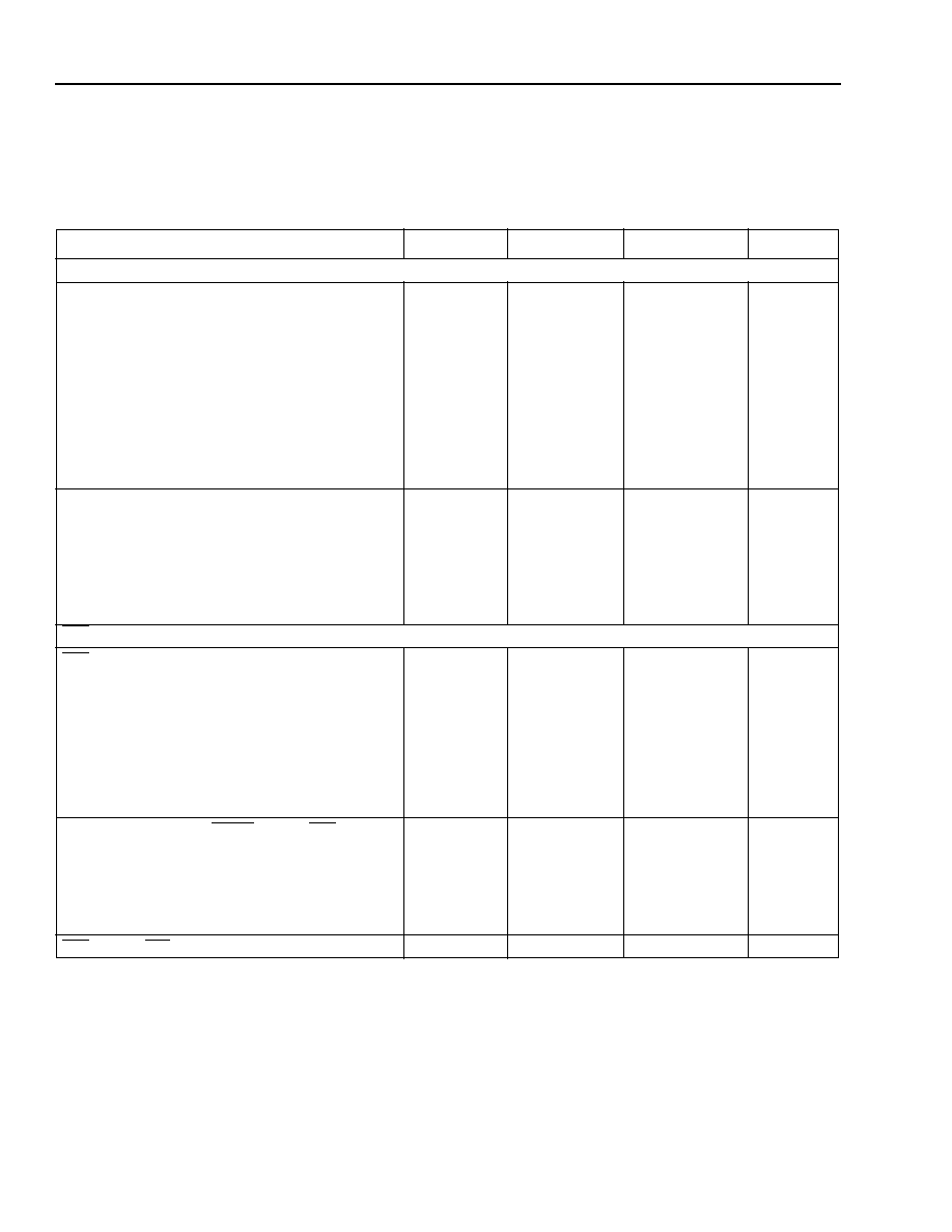
Timing Characteristics (continued)
Table 60. General Configuration Mode Timing Characteristics
(continued)
OR3Cxx Commercial: VDD = 5.0 V ± 5%, 0 °C
< TA < 70 °C; Industrial: VDD = 5.0 V ± 10%, –40 °C < TA < +85 °C.
OR3Txxx Commercial: VDD = 3.0 V to 3.6 V, 0 °C
< TA < 70 °C; Industrial: VDD = 3.0 V to 3.6 V, –40 °C < TA < +85 °C.
Note: TPO is triggered when VDD reaches between 3.0 V to 4.0 V for the OR3Cxx and between 2.7 V and 3.0 V for the OR3Txxx.
Parameter
Symbol
Min
Max
Unit
Slave Parallel Mode
Power-on Reset Delay
CCLK Period:
OR3Cxx
OR3Txxx
Conguration Latency (normal mode):
OR3T20
OR3T30
OR3T55
OR3C80
OR3T80
OR3T125
TPO
TCCLK
TCL
3.90
40.00
15.00
0.36
0.47
0.72
2.81
1.05
1.64
13.10
—
ms
ns
ms
Partial Reconguration (explicit mode):
OR3T20
OR3T30
OR3T55
OR3C80
OR3T80
OR3T125
TPR
0.48
0.54
0.65
2.04
0.77
0.93
—
s/frame
INIT
Timing
INIT
High to CCLK Delay:
Slave Parallel
Slave Serial
Master Serial:
(M3 = 1)
(M3 = 0)
Master Parallel:
(M3 = 1)
(M3 = 0)
TINIT_CCLK
1.00
0.50
4.80
1.00
—
3.40
2.00
16.20
3.60
s
Initialization Latency (PRGM high to INIT high):
OR3T20
OR3T30
OR3T55
OR3C/T80
OR3T125
TIL
0.21
0.24
0.30
0.36
0.45
0.68
0.79
1.00
1.20
1.50
ms
INIT
High to WR, Asynchronous Peripheral
TINIT_WR
2.00
—
s
Select
devices
have
been
discontinued.
See
Ordering
Information
section
for
product
status.
相關(guān)PDF資料 |
PDF描述 |
|---|---|
| OR3C804PS208-DB | FPGA, 484 CLBS, 116000 GATES, PQFP208 |
| OR3T1256PS208I-DB | FPGA, 784 CLBS, 186000 GATES, PQFP208 |
| OR3T1256PS240-DB | FPGA, 784 CLBS, 186000 GATES, PQFP240 |
| OR3T1256PS240I-DB | FPGA, 784 CLBS, 186000 GATES, PQFP240 |
| OR3T1257PS208-DB | FPGA, 784 CLBS, 186000 GATES, PQFP208 |
相關(guān)代理商/技術(shù)參數(shù) |
參數(shù)描述 |
|---|---|
| OR3C80-4BA352I | 制造商:AGERE 制造商全稱:AGERE 功能描述:3C and 3T Field-Programmable Gate Arrays |
| OR3C804BA352I-DB | 功能描述:FPGA - 現(xiàn)場可編程門陣列 3872 LUT 356 I/O RoHS:否 制造商:Altera Corporation 系列:Cyclone V E 柵極數(shù)量: 邏輯塊數(shù)量:943 內(nèi)嵌式塊RAM - EBR:1956 kbit 輸入/輸出端數(shù)量:128 最大工作頻率:800 MHz 工作電源電壓:1.1 V 最大工作溫度:+ 70 C 安裝風(fēng)格:SMD/SMT 封裝 / 箱體:FBGA-256 |
| OR3C80-4BC432 | 制造商:AGERE 制造商全稱:AGERE 功能描述:3C and 3T Field-Programmable Gate Arrays |
| OR3C80-4BC432I | 制造商:AGERE 制造商全稱:AGERE 功能描述:3C and 3T Field-Programmable Gate Arrays |
| OR3C80-4BC600I | 制造商:未知廠家 制造商全稱:未知廠家 功能描述:Field Programmable Gate Array (FPGA) |
發(fā)布緊急采購,3分鐘左右您將得到回復(fù)。