- 您現(xiàn)在的位置:買(mǎi)賣(mài)IC網(wǎng) > PDF目錄383714 > OR2T04A-4BC100 (Electronic Theatre Controls, Inc.) Field-Programmable Gate Arrays PDF資料下載
參數(shù)資料
| 型號(hào): | OR2T04A-4BC100 |
| 廠商: | Electronic Theatre Controls, Inc. |
| 元件分類(lèi): | FPGA |
| 英文描述: | Field-Programmable Gate Arrays |
| 中文描述: | 現(xiàn)場(chǎng)可編程門(mén)陣列 |
| 文件頁(yè)數(shù): | 67/192頁(yè) |
| 文件大小: | 3148K |
| 代理商: | OR2T04A-4BC100 |
第1頁(yè)第2頁(yè)第3頁(yè)第4頁(yè)第5頁(yè)第6頁(yè)第7頁(yè)第8頁(yè)第9頁(yè)第10頁(yè)第11頁(yè)第12頁(yè)第13頁(yè)第14頁(yè)第15頁(yè)第16頁(yè)第17頁(yè)第18頁(yè)第19頁(yè)第20頁(yè)第21頁(yè)第22頁(yè)第23頁(yè)第24頁(yè)第25頁(yè)第26頁(yè)第27頁(yè)第28頁(yè)第29頁(yè)第30頁(yè)第31頁(yè)第32頁(yè)第33頁(yè)第34頁(yè)第35頁(yè)第36頁(yè)第37頁(yè)第38頁(yè)第39頁(yè)第40頁(yè)第41頁(yè)第42頁(yè)第43頁(yè)第44頁(yè)第45頁(yè)第46頁(yè)第47頁(yè)第48頁(yè)第49頁(yè)第50頁(yè)第51頁(yè)第52頁(yè)第53頁(yè)第54頁(yè)第55頁(yè)第56頁(yè)第57頁(yè)第58頁(yè)第59頁(yè)第60頁(yè)第61頁(yè)第62頁(yè)第63頁(yè)第64頁(yè)第65頁(yè)第66頁(yè)當(dāng)前第67頁(yè)第68頁(yè)第69頁(yè)第70頁(yè)第71頁(yè)第72頁(yè)第73頁(yè)第74頁(yè)第75頁(yè)第76頁(yè)第77頁(yè)第78頁(yè)第79頁(yè)第80頁(yè)第81頁(yè)第82頁(yè)第83頁(yè)第84頁(yè)第85頁(yè)第86頁(yè)第87頁(yè)第88頁(yè)第89頁(yè)第90頁(yè)第91頁(yè)第92頁(yè)第93頁(yè)第94頁(yè)第95頁(yè)第96頁(yè)第97頁(yè)第98頁(yè)第99頁(yè)第100頁(yè)第101頁(yè)第102頁(yè)第103頁(yè)第104頁(yè)第105頁(yè)第106頁(yè)第107頁(yè)第108頁(yè)第109頁(yè)第110頁(yè)第111頁(yè)第112頁(yè)第113頁(yè)第114頁(yè)第115頁(yè)第116頁(yè)第117頁(yè)第118頁(yè)第119頁(yè)第120頁(yè)第121頁(yè)第122頁(yè)第123頁(yè)第124頁(yè)第125頁(yè)第126頁(yè)第127頁(yè)第128頁(yè)第129頁(yè)第130頁(yè)第131頁(yè)第132頁(yè)第133頁(yè)第134頁(yè)第135頁(yè)第136頁(yè)第137頁(yè)第138頁(yè)第139頁(yè)第140頁(yè)第141頁(yè)第142頁(yè)第143頁(yè)第144頁(yè)第145頁(yè)第146頁(yè)第147頁(yè)第148頁(yè)第149頁(yè)第150頁(yè)第151頁(yè)第152頁(yè)第153頁(yè)第154頁(yè)第155頁(yè)第156頁(yè)第157頁(yè)第158頁(yè)第159頁(yè)第160頁(yè)第161頁(yè)第162頁(yè)第163頁(yè)第164頁(yè)第165頁(yè)第166頁(yè)第167頁(yè)第168頁(yè)第169頁(yè)第170頁(yè)第171頁(yè)第172頁(yè)第173頁(yè)第174頁(yè)第175頁(yè)第176頁(yè)第177頁(yè)第178頁(yè)第179頁(yè)第180頁(yè)第181頁(yè)第182頁(yè)第183頁(yè)第184頁(yè)第185頁(yè)第186頁(yè)第187頁(yè)第188頁(yè)第189頁(yè)第190頁(yè)第191頁(yè)第192頁(yè)
Data Sheet
June 1999
ORCA Series 2 FPGAs
Lucent Technologies Inc.
67
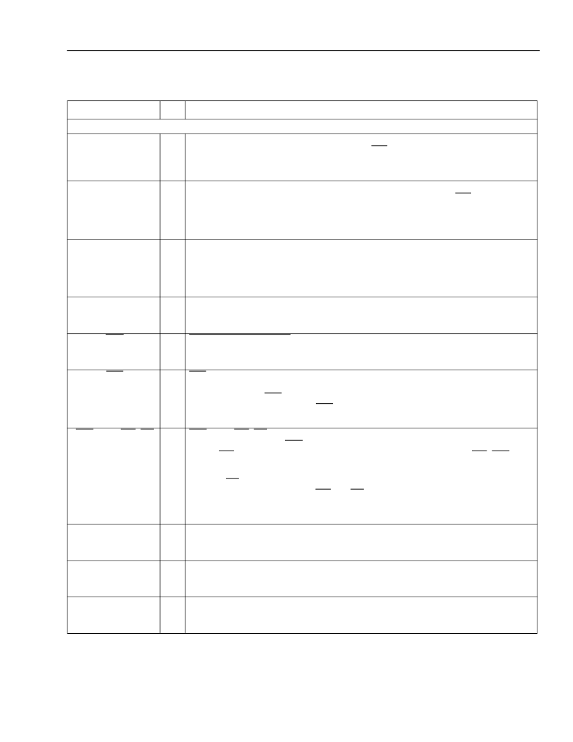
Special-Purpose Pins
Special-Purpose Pins (Become User I/O After Configuration)
(continued)
M0, M1, M2
I
During powerup and initialization, M0—M2 are used to select the configuration mode
with their values latched on the rising edge of INIT. See Table 7 for the configuration
modes. During configuration, a pull-up is enabled, and after configuration, the pins are
user-programmable I/O*.
M3
I
During powerup and initialization, M3 is used to select the speed of the internal oscilla-
tor during configuration, with its value latched on the rising edge of INIT. When M3 is
low, the oscillator frequency is 10 MHz. When M3 is high, the oscillator is 1.25 MHz.
During configuration, a pull-up is enabled, and after configuration, this pin is a user-pro-
grammable I/O pin*.
TDI, TCK, TMS
I
If boundary scan is used, these pins are Test Data In, Test Clock, and Test Mode Select
inputs. If boundary scan is not selected, all boundary-scan functions are inhibited once
configuration is complete, and these pins are user-programmable I/O pins. Even if
boundary scan is not used, either TCK or TMS must be held at logic 1 during configura-
tion. Each pin has a pull-up enabled during configuration*.
HDC
O
High During Configuration is output high until configuration is complete. It is used as a
control output indicating that configuration is not complete. After configuration, this pin is
a user-programmable I/O pin*.
LDC
O
Low During Configuration is output low until configuration is complete. It is used as a
control output indicating that configuration is not complete. After configuration, this pin is
a user-programmable I/O pin*.
INIT
I/O
INIT is a bidirectional signal before and during configuration. During configuration, a
pull-up is enabled, but an external pull-up resistor is recommended. As an active-low
open-drain output, INIT is held low during power stabilization and internal clearing of
memory. As an active-low input, INIT holds the FPGA in the wait-state before the start of
configuration. After configuration, the pin is a user-programmable I/O pin*.
CS0, CS1, WR, RD
I
CS0, CS1, WR, RD are used in the asynchronous peripheral configuration modes. The
FPGA is selected when CS0 is low and CS1 is high. When selected, a low on the write
strobe, WR, loads the data on D[7:0] inputs into an internal data buffer. WR, CS0, and
CS1 are also used as chip selects in the slave parallel mode.
A low on RD changes D7 into a status output. As a status indication, a high indicates
ready and a low indicates busy. WR and RD should not be used simultaneously. If they
are, the write strobe overrides. During configuration, a pull-up is enabled, and after con-
figuration, the pins are user-programmable I/O pins*.
During master parallel configuration mode, A[17:0] address the configuration EPROM.
During configuration, a pull-up is enabled, and after configuration, the pins are user-
programmable I/O pins*.
During master parallel, peripheral, and slave parallel configuration modes, D[7:0]
receive configuration data and each pin has a pull-up enabled. After configuration, the
pins are user-programmable I/O pins*.
During configuration, DOUT is the serial data output that can drive the DIN of daisy-
chained slave LCA devices. Data out on DOUT changes on the falling edge of CCLK.
After configuration, DOUT is a user-programmable I/O pin*.
A[17:0]
O
D[7:0]
I
DOUT
O
Table 17. Pin Descriptions
(continued)
Symbol
I/O
Description
* The FPGA States of Operation section contains more information on how to control these signals during start-up. The timing of DONE
release is controlled by one set of bit stream options, and the timing of the simultaneous release of all other configuration pins (and the acti-
vation of all user I/Os) is controlled by a second set of options.
Pin Information
(continued)
相關(guān)PDF資料 |
PDF描述 |
|---|---|
| OR2T04A-4BC100I | Field-Programmable Gate Arrays |
| OR2T04A-4BC144 | Field-Programmable Gate Arrays |
| OR2T04A-4BC144I | Ceramic Chip Capacitors / MIL-PRF-55681; Capacitance [nom]: 1000pF; Working Voltage (Vdc)[max]: 100V; Capacitance Tolerance: +/-1%; Dielectric: Multilayer Ceramic; Temperature Coefficient: C0G (NP0); Lead Style: Surface Mount Chip; Lead Dimensions: 1206; Termination: Solder Coated SnPb; Body Dimensions: 0.125" x 0.062" x 0.051"; Container: Bag; Features: MIL-PRF-55681: M Failure Rate |
| OR2T04A-4BC160 | Field-Programmable Gate Arrays |
| OR2T04A-4BC160I | Field-Programmable Gate Arrays |
相關(guān)代理商/技術(shù)參數(shù) |
參數(shù)描述 |
|---|---|
| OR2T04A-4BC100I | 制造商:未知廠家 制造商全稱(chēng):未知廠家 功能描述:Field-Programmable Gate Arrays |
| OR2T04A-4BC144 | 制造商:未知廠家 制造商全稱(chēng):未知廠家 功能描述:Field-Programmable Gate Arrays |
| OR2T04A-4BC144I | 制造商:未知廠家 制造商全稱(chēng):未知廠家 功能描述:Field-Programmable Gate Arrays |
| OR2T04A-4BC160 | 制造商:未知廠家 制造商全稱(chēng):未知廠家 功能描述:Field-Programmable Gate Arrays |
| OR2T04A-4BC160I | 制造商:未知廠家 制造商全稱(chēng):未知廠家 功能描述:Field-Programmable Gate Arrays |
發(fā)布緊急采購(gòu),3分鐘左右您將得到回復(fù)。