- 您現(xiàn)在的位置:買賣IC網(wǎng) > PDF目錄383693 > OPA699IDR Wideband, High Gain VOLTAGE LIMITING AMPLIFIER PDF資料下載
參數(shù)資料
| 型號: | OPA699IDR |
| 元件分類: | 運動控制電子 |
| 英文描述: | Wideband, High Gain VOLTAGE LIMITING AMPLIFIER |
| 中文描述: | 寬帶,高增益電壓限幅放大器 |
| 文件頁數(shù): | 20/25頁 |
| 文件大?。?/td> | 461K |
| 代理商: | OPA699IDR |
OPA699
SBOS261B
20
www.ti.com
When the limiter voltages are more than 2.1V from the
supplies (V
L
≥
–
V
S
+ 2.1V or V
H
≤
+V
S
–
2.1V), you can use
simple resistor dividers to set V
H
and V
L
(see Figure 1). Make
sure to include the limiter input bias currents (Figure 8) in the
calculations (that is, I
VL
= 50
μ
A into pin 5, and I
VH
= +50
μ
A
out of pin 8). For good limiter voltage accuracy, run a
minimum 1mA quiescent bias current through these resis-
tors. When the limiter voltages need to be within 2.1V of the
supplies (V
L
≤
–
V
S
+ 2.1V or V
H
≥
+V
S
–
2.1V), consider using
low impedance buffers to set V
H
and V
L
to minimize errors
due to bias current uncertainty. This condition will typically be
the case for single-supply operation (V
S
= +5V). Figure 2
runs 2.5mA through the resistive divider that sets V
H
and V
L
.
This limits errors due to I
VH
and I
VL
<
±
1% of the target limit
voltages. The limiters
’
DC accuracy depends on attention to
detail. The two dominant error sources can be improved as
follows:
Power supplies, when used to drive resistive dividers that
set V
H
and V
L
, can contribute large errors (for example,
±
5%). Using a more accurate source, and bypassing pins
5 and 8 with good capacitors, will improve limiter PSRR.
The resistor tolerances in the resistive divider can also
dominate. Use 1% resistors.
Other error sources also contribute, but should have little
impact on the limiters
’
DC accuracy:
Reduce offsets caused by the Limiter Input Bias Currents.
Select the resistors in the resistive divider(s) as described
above.
Consider the signal path DC errors as contributing to
uncertainty in the useable output swing.
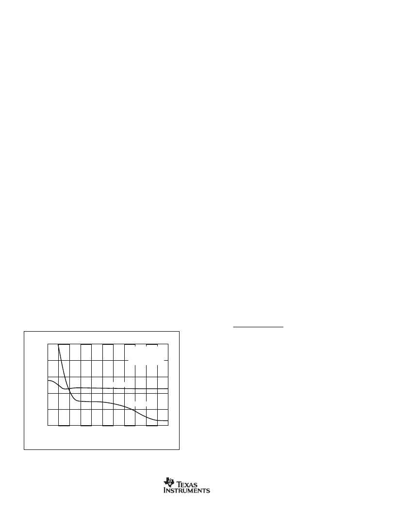
The limiter offset voltage only slightly degrades limiter
accuracy. Figure 13 shows how the limiters affect distor-
tion performance. Virtually no degradation in linearity is
observed for output voltage swinging right up to the limiter
voltages. In this plot a fixed
±
1V output swing is driven
while the limiter voltages are reduced symmetrically. Until
the limiters are reduced to
±
1.1V, little distortion degrada-
tion is observed.
OUTPUT DRIVE
The OPA699 has been optimized to drive 500
loads, such
as ADCs. It still performs very well driving 100
loads; the
specifications are shown for the 500
load. This makes the
OPA699 an ideal choice for a wide range of high-frequency
applications.
Many high-speed applications, such as driving ADCs, require
op amps with low output impedance. As shown in the typical
performance curve Output Impedance vs Frequency the
OPA699 maintains very low closed-loop output impedance
over frequency. Closed-loop output impedance increases
with frequency, since loop gain decreases with frequency.
THERMAL CONSIDERATIONS
The OPA699 will not require heat sinking under most oper-
ating conditions. Maximum desired junction temperature will
set a maximum allowed internal power dissipation as de-
scribed below. In no case should the maximum junction
temperature be allowed to exceed 150
°
C.
The total internal power dissipation (P
D
) is the sum of
quiescent power (P
DQ
) and the additional power dissipated in
the output stage (P
DL
) while delivering load power. P
DQ
is
simply the specified no-load supply current times the total
supply voltage across the part. P
DL
depends on the required
output signals and loads. For a grounded resistive load, and
equal bipolar supplies, it is at maximum when the output is
at 1/2 either supply voltage. In this condition, P
DL
= V
S2
/(4R
L
)
where R
L
includes the feedback network loading. Note that it
is the power in the output stage, and not in the load, that
determines internal power dissipation.
The operating junction temperature is: T
J
= T
A
+ P
D
x
θ
JA
,
where T
A
is the ambient temperature. For example, the
maximum T
J
for a OPA699ID with G = +6, R
F
= 750
,
R
L
= 500
, and
±
V
S
=
±
5V at the maximum T
A
= +85
°
C is
calculated as:
P
V
mA
mW
P
V
mW
P
T
mW
C
°
85
mW
mW
mW
C W
°
/
C
DQ
DL
D
J
=
×
(
)
=
=
(
)
×
(
)
=
=
=
+
=
125
+
×
=
°
10
15 5
155
5
4
500
900
19 4
155
19 4
.
174 4
174 4
107
2
.
||
.
.
.
This would be the maximum T
J
from V
O
=
±
2.5V
DC
. Most
applications will be at a lower output stage power and have
a lower T
J
.
CAPACITIVE LOADS
Capacitive loads, such as the input to ADCs, will decrease
the amplifier phase margin, which may cause high-frequency
peaking or oscillations. Capacitive loads
≥
2pF should be
isolated by connecting a small resistor in series with the
output, as shown in Figure 14. Increasing the gain from +2
will improve the capacitive drive capabilities due to increased
phase margin.
H
±
Limit Voltage (V)
0.9
1.0
1.1
1.2
1.3
1.4
1.5
1.6
1.7 1.8
1.9
2.0
40
50
60
70
80
90
3rd-Harmonic
2nd-Harmonic
V
= 0V
DC
±
1V
P
f = 5MHz
R
L
= 500
FIGURE 13. Harmonic Distortion Near Limit Voltages.
相關(guān)PDF資料 |
PDF描述 |
|---|---|
| OPA708 | REFLECTIVE OBJECT SENSORS |
| OPA729 | 10 Watt Light Bar on Anotherm Linear Heat Spreader |
| OPA729B | 10 Watt Light Bar on Anotherm Linear Heat Spreader |
| OPA729BD | 10 Watt Light Bar on Anotherm Linear Heat Spreader |
| OPA729G | 10 Watt Light Bar on Anotherm Linear Heat Spreader |
相關(guān)代理商/技術(shù)參數(shù) |
參數(shù)描述 |
|---|---|
| OPA699IDRG4 | 功能描述:高速運算放大器 Wideband High Gain Vltg Limiting RoHS:否 制造商:Texas Instruments 通道數(shù)量:1 電壓增益 dB:116 dB 輸入補償電壓:0.5 mV 轉(zhuǎn)換速度:55 V/us 工作電源電壓:36 V 電源電流:7.5 mA 最大工作溫度:+ 85 C 安裝風(fēng)格:SMD/SMT 封裝 / 箱體:SOIC-8 封裝:Tube |
| OPA699M | 制造商:TI 制造商全稱:Texas Instruments 功能描述:GAIN 4 STABLE WIDEBAND VOLTAGE LIMITING AMPLIFIER |
| OPA699MJD | 制造商:Texas Instruments 功能描述:OP Amp Single Volt Fdbk ±6V/12V 8-Pin SBCDIP Tube |
| OPA703 | 制造商:TI 制造商全稱:Texas Instruments 功能描述:CMOS, Rail-to-Rail, I/O OPERATIONAL AMPLIFIERS |
| OPA703_08 | 制造商:BB 制造商全稱:BB 功能描述:CMOS, Rail-to-Rail, I/O OPERATIONAL AMPLIFIERS |
發(fā)布緊急采購,3分鐘左右您將得到回復(fù)。