- 您現(xiàn)在的位置:買賣IC網(wǎng) > PDF目錄383693 > OPA699IDR Wideband, High Gain VOLTAGE LIMITING AMPLIFIER PDF資料下載
參數(shù)資料
| 型號: | OPA699IDR |
| 元件分類: | 運動控制電子 |
| 英文描述: | Wideband, High Gain VOLTAGE LIMITING AMPLIFIER |
| 中文描述: | 寬帶,高增益電壓限幅放大器 |
| 文件頁數(shù): | 15/25頁 |
| 文件大?。?/td> | 461K |
| 代理商: | OPA699IDR |
OPA699
SBOS261B
15
www.ti.com
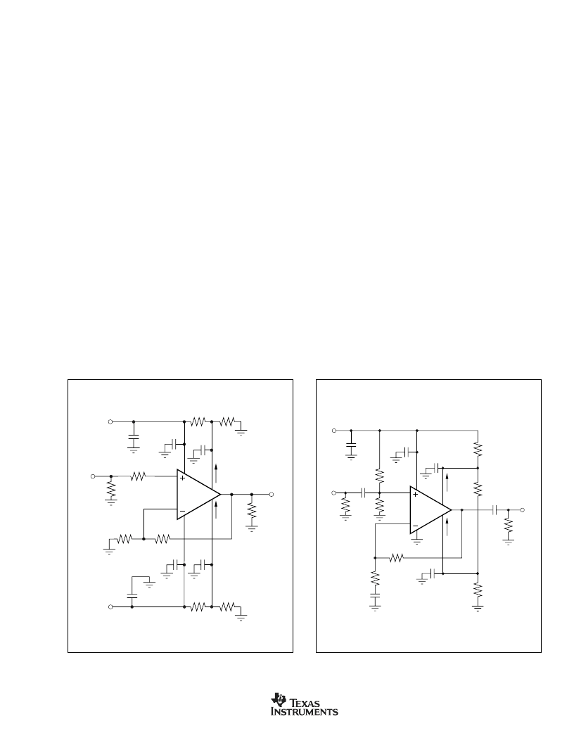
TYPICAL APPLICATIONS
WIDEBAND VOLTAGE LIMITING OPERATION
The OPA699 is a gain voltage of +4V/V, voltage-feedback
amplifier that combines features of a wideband, high slew
rate amplifier with output voltage limiters. Its output can
swing up to 1V from each rail and can deliver up to 120mA.
These capabilities make it an ideal interface to drive an ADC
while adding overdrive protection for the ADC inputs.
Figure 1 shows the DC-coupled, gain of +6V/V, dual power-
supply circuit configuration used as the basis of the
±
5V
Electrical Characteristics and Typical Characteristics. For
test purposes, the input impedance is set to 50
with a
resistor to ground and the output is set to 500
. Voltage
swings reported in the specifications are taken directly at the
input and output pins. For the circuit of Figure 1, the total
output load will be 500
|| 900
= 321
. The voltage limiting
pins are set to
±
2V through a voltage divider network be-
tween the +V
S
and ground for V
H
, and between
–
V
S
and ground for V
L
. These limiter voltages are adequately
bypassed with a 0.1
μ
F ceramic capacitor to ground. The
limiter voltages (V
H
and V
L
) and the respective bias currents
(I
VH
and I
VL
) have the polarities shown. One additional
component is included in Figure 1. An additional resistor
(100
) is included in series with the noninverting input.
Combined with the 25
DC source resistance looking back
towards the signal generator, this gives an input bias current-
canceling resistance that matches the 125
source resis-
tance seen at the inverting input (see the DC accuracy and
offset control section). The power-supply bypass for each
supply consists of two capacitors: one electrolytic 2.2
μ
F and
one ceramic 0.1
μ
F. The power-supply bypass capacitors are
shown explicitly in Figures 1 and 2, but will be assumed in the
other figures. An additional 0.01
μ
F power-supply decoupling
capacitor (not shown here) can be included between the
two power-supply pins. In practical PC board layouts, this
optional, added capacitor will typically improve the 2nd
harmonic distortion performance by 3dB to 6dB.
SINGLE-SUPPLY, NONINVERTING AMPLIFIER
Figure 2 shows an AC-coupled, noninverting gain amplifier
for single +5V supply operation. This circuit was used for AC
characterization of the OPA699, with a 50
source (which it
matches) and a 500
load. The mid-point reference on the
noninverting input is set by two 1.5k
resistors. This gives an
input bias current-canceling resistance that matches the
750
DC source resistance seen at the inverting input (see
the DC accuracy and offset control section). The power-
supply bypass for the supply consists of two capacitors: one
electrolytic 2.2
μ
F and one ceramic 0.1
μ
F. The power-supply
bypass capacitors are shown explicitly in Figures 1 and 2, but
will be assumed in the other figures. The limiter voltages (V
H
and V
L
) and the respective bias currents (I
VH
and I
VL
) have
the polarities shown. These limiter voltages are adequately
bypassed with a 0.1
μ
F ceramic capacitor to ground. Notice
that the single-supply circuit can use three resistors to set V
H
and V
L
, where the dual-supply circuit usually uses four to
reference the limit voltages to ground. While this circuit
shows +5V operation, the same circuit may be used for
single supplies up to +12V.
OPA699
49.9
6
I
VH
V
O
V
IN
I
VL
–
V
S
=
–
5V
3
2
4
7
8
5
R
F
750
R
G
150
500
0.1
μ
F
0.1
μ
F
0.1
μ
F
100
3.01k
1.91k
3.01k
1.91k
0.1
μ
F
V
H
= +2V
V
L
=
–
2V
+
2.2
μ
F
+
2.2
μ
F
+V
S
= +5V
OPA699
53.6
6
I
VH
V
H
= 3.7V
V
O
V
L
= 1.3V
V
IN
I
VL
1.5k
3
2
4
7
8
5
1.5k
523
976
523
R
G
150
R
F
750
500
0.1
μ
F
0.1
μ
F
0.1
μ
F
+
2.2
μ
F
0.1
μ
F
V
S
= +5V
0.1
μ
F
0.1
μ
F
FIGURE 1. DC-Coupled, Dual-Supply Amplifier.
FIGURE 2. AC-Coupled, Single-Supply Amplifier.
相關(guān)PDF資料 |
PDF描述 |
|---|---|
| OPA708 | REFLECTIVE OBJECT SENSORS |
| OPA729 | 10 Watt Light Bar on Anotherm Linear Heat Spreader |
| OPA729B | 10 Watt Light Bar on Anotherm Linear Heat Spreader |
| OPA729BD | 10 Watt Light Bar on Anotherm Linear Heat Spreader |
| OPA729G | 10 Watt Light Bar on Anotherm Linear Heat Spreader |
相關(guān)代理商/技術(shù)參數(shù) |
參數(shù)描述 |
|---|---|
| OPA699IDRG4 | 功能描述:高速運算放大器 Wideband High Gain Vltg Limiting RoHS:否 制造商:Texas Instruments 通道數(shù)量:1 電壓增益 dB:116 dB 輸入補償電壓:0.5 mV 轉(zhuǎn)換速度:55 V/us 工作電源電壓:36 V 電源電流:7.5 mA 最大工作溫度:+ 85 C 安裝風(fēng)格:SMD/SMT 封裝 / 箱體:SOIC-8 封裝:Tube |
| OPA699M | 制造商:TI 制造商全稱:Texas Instruments 功能描述:GAIN 4 STABLE WIDEBAND VOLTAGE LIMITING AMPLIFIER |
| OPA699MJD | 制造商:Texas Instruments 功能描述:OP Amp Single Volt Fdbk ±6V/12V 8-Pin SBCDIP Tube |
| OPA703 | 制造商:TI 制造商全稱:Texas Instruments 功能描述:CMOS, Rail-to-Rail, I/O OPERATIONAL AMPLIFIERS |
| OPA703_08 | 制造商:BB 制造商全稱:BB 功能描述:CMOS, Rail-to-Rail, I/O OPERATIONAL AMPLIFIERS |
發(fā)布緊急采購,3分鐘左右您將得到回復(fù)。