- 您現(xiàn)在的位置:買賣IC網(wǎng) > PDF目錄383693 > OPA683IDBVR OP-AMP|SINGLE|BIPOLAR|TSOP|6PIN|PLASTIC PDF資料下載
參數(shù)資料
| 型號(hào): | OPA683IDBVR |
| 元件分類: | 運(yùn)動(dòng)控制電子 |
| 英文描述: | OP-AMP|SINGLE|BIPOLAR|TSOP|6PIN|PLASTIC |
| 中文描述: | 運(yùn)放|單|雙極|的TSOP | 6針|塑料 |
| 文件頁數(shù): | 18/24頁 |
| 文件大?。?/td> | 400K |
| 代理商: | OPA683IDBVR |
OPA683
SBOS221B
18
www.ti.com
cludes the feedback network
—
in the noninverting configura-
tion (see Figure 1) this is the sum of R
F
+ R
G
, while in the
inverting configuration it is just R
F
. Also, providing an addi-
tional supply decoupling capacitor (0.1
μ
F) between the sup-
ply pins (for bipolar operation) improves the 2nd-order distor-
tion slightly (3dB to 6dB).
In most op amps, increasing the output voltage swing in-
creases harmonic distortion directly. A low-power part like the
OPA683 includes quiescent boost circuits to provide the full-
power bandwidth shown. These act to increase the bias in a
very linear fashion only when high slew rate or output power
are required. The Typical Characteristics show the 2nd-har-
monic increasing slightly from 500mVp-p to 5Vp-p outputs
while the 3rd-harmonics also increase with output power.
The OPA683 has an extremely low 3rd-order harmonic distor-
tion
—
particularly for light loads and at lower frequencies. This
also gives low 2-tone, 3rd-order intermodulation distortion as
shown in the Typical Characteristics. Since the OPA683
includes internal power boost circuits to retain good full-power
performance at high frequencies and outputs, it does not show
a classical 2-tone, 3rd-order intermodulation intercept charac-
teristic. Instead, it holds relatively low and constant 3rd-order
intermodulation spurious levels over power. The Typical Char-
acteristics show this spurious level as a dBc below the carrier
at fixed center frequencies swept over single-tone voltage
swing at a 1k
load. Very light loads such as ADC inputs for
will see <
–
85dBc 3rd-order spurious to 1MHz for full-scale
inputs. For much lower 3rd-order intermodulation distortion
through 200MHz, consider the OPA685.
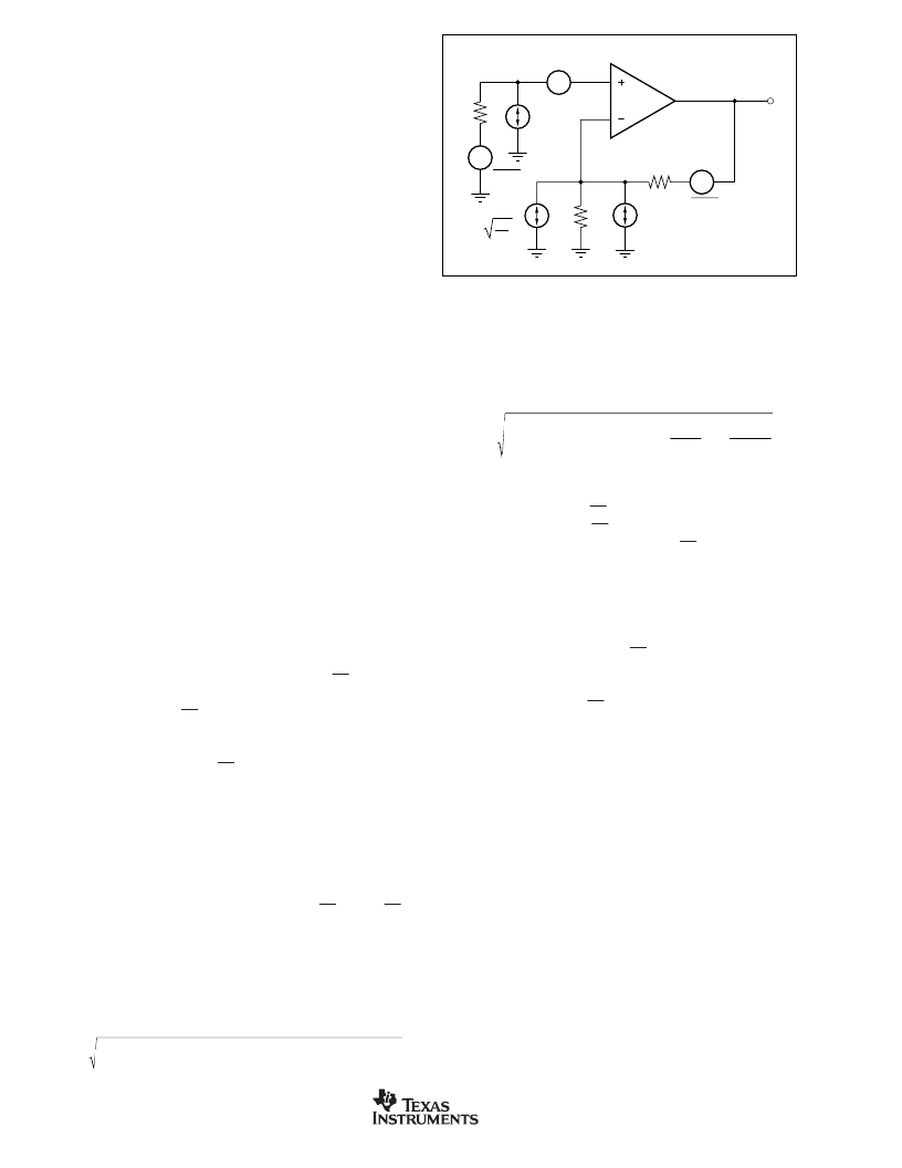
NOISE PERFORMANCE
Wideband current-feedback op amps generally have a higher
output noise than comparable voltage feedback op amps. The
OPA683 offers an excellent balance between voltage and
current noise terms to achieve low output noise in a low- power
amplifier. The inverting current noise (11.6pA/
√
Hz
) is lower
than most other current feedback op amps while the input
voltage noise (4.4nV/
√
Hz
) is lower than any unity-gain stable,
comparable slew rate, voltage feedback op amp. This low input
voltage noise was achieved at the price of higher noninverting
input current noise (5.1pA/
√
Hz
). As long as the AC source
impedance looking out of the noninverting node is less than
300
, this current noise will not contribute significantly to the
total output noise. The op amp input voltage noise and the two
input current noise terms combine to give low output noise
under a wide variety of operating conditions. Figure 13 shows
the op amp noise analysis model with all the noise terms
included. In this model, all noise terms are taken to be noise
voltage or current density terms in either nV/
√
Hz
or pA/
√
Hz
.
The total output spot noise voltage can be computed as the
square root of the sum of all squared output noise voltage
contributors. Equation 3 shows the general form for the
output noise voltage using the terms shown in Figure 13.
(3)
E
E
I
R
kTR
4
G
I R
kTR G
4
O
NI
BN
S
S
N
N
=
+
(
)
+
+
(
)
+
2
2
2
2
4kT
R
G
R
G
R
F
R
S
OPA683
I
BI
E
O
I
BN
4kT = 1.6E
–
20J
at 290
°
K
E
RS
E
NI
4kTR
S
√
4kTR
F
√
Dividing this expression by the noise gain (NG = (1 + R
F
/R
G
))
will give the equivalent input referred spot noise voltage at the
noninverting input, as shown in Equation 4.
(4)
E
E
I
R
kTR
4
I R
G
kTR
G
N
NI
BN
S
S
N
F
N
=
+
(
)
+
+
+
2
2
2
4
Evaluating these two equations for the OPA683 circuit and
component values (see Figure 1) will give a total output spot
noise voltage of 17.6nV/
√
Hz
and a total equivalent input spot
noise voltage of 8.8nV/
√
Hz
. This total input referred spot
noise voltage is higher than the 4.4nV/
√
Hz
specification for
the op amp voltage noise alone. This reflects the noise
added to the output by the inverting current noise times the
feedback resistor. As the gain is increased, this fixed output
noise power term contributes less to the total output noise
and the total input referred voltage noise given by Equation
3 will approach just the 4.4nV/
√
Hz
of the op amp itself. For
example, going to a gain of +20 in the circuit of Figure 1,
adjusting only the gain resistor to 63.2
, will give a total input
referred noise of 4.6nV/
√
Hz
. A more complete description of
op amp noise analysis can be found in the TI application note
AB-103 (SBOA066). Refer to Texas Instruments
’
web site
www.ti.com.
DC ACCURACY AND OFFSET CONTROL
A current-feedback op amp like the OPA683 provides excep-
tional bandwidth in high gains, giving fast pulse settling but
only moderate DC accuracy. The Electrical Characteristics
show an input offset voltage comparable to high slew rate
voltage-feedback amplifiers. However, the two input bias
currents are somewhat higher and are unmatched. Whereas
bias current cancellation techniques are very effective with
most voltage feedback op amps, they do not generally
reduce the output DC offset for wideband current-feedback
op amps. Since the two input bias currents are unrelated in
both magnitude and polarity, matching the source imped-
ance looking out of each input to reduce their error contribu-
tion to the output is ineffective. Evaluating the configuration
of Figure 1, using worst case +25
°
C input offset voltage and
FIGURE 13. Op Amp Noise Analysis Model.
相關(guān)PDF資料 |
PDF描述 |
|---|---|
| OPA683IDBVT | OP-AMP|SINGLE|BIPOLAR|TSOP|6PIN|PLASTIC |
| OPA683IDR | OP-AMP|SINGLE|BIPOLAR|SOP|8PIN|PLASTIC |
| OPA685 | Ultra-Wideband, Current-Feedback OPERATIONAL AMPLIFIER With Disable TM |
| OPA685N | Ultra-Wideband, Current-Feedback OPERATIONAL AMPLIFIER With Disable TM |
| OPA685U | Ultra-Wideband, Current-Feedback OPERATIONAL AMPLIFIER With Disable TM |
相關(guān)代理商/技術(shù)參數(shù) |
參數(shù)描述 |
|---|---|
| OPA683IDBVRG4 | 功能描述:高速運(yùn)算放大器 Very Lo-Pwr Current Feedback RoHS:否 制造商:Texas Instruments 通道數(shù)量:1 電壓增益 dB:116 dB 輸入補(bǔ)償電壓:0.5 mV 轉(zhuǎn)換速度:55 V/us 工作電源電壓:36 V 電源電流:7.5 mA 最大工作溫度:+ 85 C 安裝風(fēng)格:SMD/SMT 封裝 / 箱體:SOIC-8 封裝:Tube |
| OPA683IDBVT | 功能描述:高速運(yùn)算放大器 Very Lo-Pwr Current Feedback RoHS:否 制造商:Texas Instruments 通道數(shù)量:1 電壓增益 dB:116 dB 輸入補(bǔ)償電壓:0.5 mV 轉(zhuǎn)換速度:55 V/us 工作電源電壓:36 V 電源電流:7.5 mA 最大工作溫度:+ 85 C 安裝風(fēng)格:SMD/SMT 封裝 / 箱體:SOIC-8 封裝:Tube |
| OPA683IDBVTG4 | 功能描述:高速運(yùn)算放大器 Very Lo-Pwr Current Feedback RoHS:否 制造商:Texas Instruments 通道數(shù)量:1 電壓增益 dB:116 dB 輸入補(bǔ)償電壓:0.5 mV 轉(zhuǎn)換速度:55 V/us 工作電源電壓:36 V 電源電流:7.5 mA 最大工作溫度:+ 85 C 安裝風(fēng)格:SMD/SMT 封裝 / 箱體:SOIC-8 封裝:Tube |
| OPA683IDG4 | 功能描述:高速運(yùn)算放大器 Very Lo-Pwr Current Feedback RoHS:否 制造商:Texas Instruments 通道數(shù)量:1 電壓增益 dB:116 dB 輸入補(bǔ)償電壓:0.5 mV 轉(zhuǎn)換速度:55 V/us 工作電源電壓:36 V 電源電流:7.5 mA 最大工作溫度:+ 85 C 安裝風(fēng)格:SMD/SMT 封裝 / 箱體:SOIC-8 封裝:Tube |
| OPA683IDR | 功能描述:高速運(yùn)算放大器 Very Lo-Pwr Current Feedback RoHS:否 制造商:Texas Instruments 通道數(shù)量:1 電壓增益 dB:116 dB 輸入補(bǔ)償電壓:0.5 mV 轉(zhuǎn)換速度:55 V/us 工作電源電壓:36 V 電源電流:7.5 mA 最大工作溫度:+ 85 C 安裝風(fēng)格:SMD/SMT 封裝 / 箱體:SOIC-8 封裝:Tube |
發(fā)布緊急采購,3分鐘左右您將得到回復(fù)。