- 您現(xiàn)在的位置:買賣IC網(wǎng) > PDF目錄383693 > OPA683IDBVR OP-AMP|SINGLE|BIPOLAR|TSOP|6PIN|PLASTIC PDF資料下載
參數(shù)資料
| 型號: | OPA683IDBVR |
| 元件分類: | 運動控制電子 |
| 英文描述: | OP-AMP|SINGLE|BIPOLAR|TSOP|6PIN|PLASTIC |
| 中文描述: | 運放|單|雙極|的TSOP | 6針|塑料 |
| 文件頁數(shù): | 12/24頁 |
| 文件大小: | 400K |
| 代理商: | OPA683IDBVR |
OPA683
SBOS221B
12
www.ti.com
APPLICATIONS INFORMATION
VERY LOW POWER CURRENT-FEEDBACK
OPERATION
The OPA683 gives a new level of performance in very low
power current-feedback op amps. Using a new input stage
buffer architecture, the OPA683 CFB
plus
amplifier gives im-
proved bandwidth to higher gains than previous < 1mA
supply current amplifiers. This closed-loop internal buffer
gives a very low and linearized impedance at the inverting
node
—
isolating the amplifier
’
s AC performance from gain
element variations. This allows both the bandwidth and
distortion to remain nearly constant over gain
—
moving closer
to the ideal current-feedback performance of Gain Bandwidth
independence. This low power amplifier also delivers excep-
tional output power
—
it
’
s
±
4V swing on
±
5V supplies with
> 100mA output drive gives excellent performance into
standard video loads or doubly-terminated 50
cables. Single
+5V supply operation is also supported with similar band-
widths, but reduced output power capability. For improved
harmonic distortion driving heavier loads, in a low power
CFB
plus
amplifier, consider the OPA684 while, for even
higher output power, consider the OPA691.
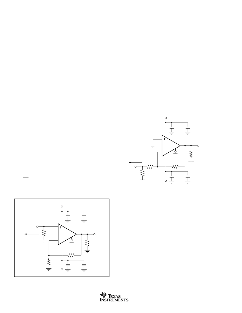
Figure 1 shows the DC-coupled, gain of +2, dual power-
supply circuit used as the basis of the
±
5V Electrical Charac-
teristics and Typical Characteristics. For test purposes, the
input impedance is set to 50
with a resistor to ground while
the output load is a 1k
resistor. Voltage swings reported in
the specifications are taken directly at the input and output
pins while load powers (dBm) are interpreted as the voltage
swing at the output converted to dBm as if the load were
50
. For the circuit of Figure 1, the total effective load will be
1k
|| 2.4k
= 706
. Gain changes are most easily accom-
plished by simply resetting the R
G
value
—
holding R
F
con-
stant at its recommended value of 1.2k
. The disable control
line (
DIS
) is typically left open to ensure normal amplifier
operation. It may, however, be asserted LOW to reduce the
amplifier quiescent to 100
μ
A typically.
Figure 2 shows the DC-coupled, gain of
–
1V/V, dual power-
supply circuit used as the basis of the Inverting Typical
Characteristics. Inverting operation offers several perfor-
mance benefits. Since there is no common-mode signal
across the input stage, the slew rate for inverting operation
is higher and the distortion performance is slightly improved.
An additional input resistor, R
M
, is included in Figure 2 to set
the input impedance equal to the 50
. The parallel combina-
tion of R
M
and R
G
set the input impedance. As the desired
gain increases for the inverting configuration, R
G
is adjusted
to achieved the desired gain and R
M
is also adjusted to hold
a 50
input match. A point will be reached where R
G
will
equal 50
, R
M
is then removed and the input match is set by
R
G
only. With R
G
fixed to achieve an input match to 50
, to
increase gain, R
F
is simply increased. This will, however,
quickly reduce the achievable bandwidth as the feedback
resistor increases from its recommended value of 1.2k
. If
the source does not require an input match to 50
, either
adjust R
M
to the get the desired load or remove it and let the
R
G
resistor alone provide the input load.
R
F
1.2k
V
O
OPA683
+5V
–
5V
DIS
1k
50
R
1.2k
R
G
=
50
V
I
0.1
μ
F
6.8
μ
F
0.1
μ
F
6.8
μ
F
+
+
FIGURE 1. DC-Coupled, G = +2V/V, Bipolar Supply, Speci-
fication and Test Circuit.
FIGURE 2. DC-Coupled, G =
–
1V/V, Bipolar Supply, Speci-
fication and Test Circuit.
R
F
1.2k
OPA683
+5V
–
5V
DIS
R
52.3
R
G
1.2k
R
S
=
50
0.1
μ
F
6.8
μ
F
0.1
μ
F
6.8
μ
F
+
+
V
I
V
O
1k
These circuits are showing
±
5V operation. The same circuit
can be applied with bipolar supplies ranging from
±
2.5V to
±
6V. Internal supply independent biasing gives nearly the
same performance for the OPA683 over this wide range of
supplies. Generally, the optimum feedback resistor value (for
nominally flat frequency response at G = +2) will increase in
value as the total supply voltage across the OPA683 is
reduced.
See Figure 3 for the AC-coupled, single +5V supply, gain of
+2V/V circuit configuration used as a basis for the +5V only
Electrical Characteristics and Typical Characteristics. The
key requirement of broadband single-supply operation is to
maintain input and output signal swings within the usable
voltage ranges at both the input and the output. The circuit
of Figure 3 establishes an input midpoint bias using a simple
resistive divider from the +5V supply (two 12.5k
resistors)
to the noninverting input. The input signal is then AC-coupled
相關(guān)PDF資料 |
PDF描述 |
|---|---|
| OPA683IDBVT | OP-AMP|SINGLE|BIPOLAR|TSOP|6PIN|PLASTIC |
| OPA683IDR | OP-AMP|SINGLE|BIPOLAR|SOP|8PIN|PLASTIC |
| OPA685 | Ultra-Wideband, Current-Feedback OPERATIONAL AMPLIFIER With Disable TM |
| OPA685N | Ultra-Wideband, Current-Feedback OPERATIONAL AMPLIFIER With Disable TM |
| OPA685U | Ultra-Wideband, Current-Feedback OPERATIONAL AMPLIFIER With Disable TM |
相關(guān)代理商/技術(shù)參數(shù) |
參數(shù)描述 |
|---|---|
| OPA683IDBVRG4 | 功能描述:高速運算放大器 Very Lo-Pwr Current Feedback RoHS:否 制造商:Texas Instruments 通道數(shù)量:1 電壓增益 dB:116 dB 輸入補償電壓:0.5 mV 轉(zhuǎn)換速度:55 V/us 工作電源電壓:36 V 電源電流:7.5 mA 最大工作溫度:+ 85 C 安裝風格:SMD/SMT 封裝 / 箱體:SOIC-8 封裝:Tube |
| OPA683IDBVT | 功能描述:高速運算放大器 Very Lo-Pwr Current Feedback RoHS:否 制造商:Texas Instruments 通道數(shù)量:1 電壓增益 dB:116 dB 輸入補償電壓:0.5 mV 轉(zhuǎn)換速度:55 V/us 工作電源電壓:36 V 電源電流:7.5 mA 最大工作溫度:+ 85 C 安裝風格:SMD/SMT 封裝 / 箱體:SOIC-8 封裝:Tube |
| OPA683IDBVTG4 | 功能描述:高速運算放大器 Very Lo-Pwr Current Feedback RoHS:否 制造商:Texas Instruments 通道數(shù)量:1 電壓增益 dB:116 dB 輸入補償電壓:0.5 mV 轉(zhuǎn)換速度:55 V/us 工作電源電壓:36 V 電源電流:7.5 mA 最大工作溫度:+ 85 C 安裝風格:SMD/SMT 封裝 / 箱體:SOIC-8 封裝:Tube |
| OPA683IDG4 | 功能描述:高速運算放大器 Very Lo-Pwr Current Feedback RoHS:否 制造商:Texas Instruments 通道數(shù)量:1 電壓增益 dB:116 dB 輸入補償電壓:0.5 mV 轉(zhuǎn)換速度:55 V/us 工作電源電壓:36 V 電源電流:7.5 mA 最大工作溫度:+ 85 C 安裝風格:SMD/SMT 封裝 / 箱體:SOIC-8 封裝:Tube |
| OPA683IDR | 功能描述:高速運算放大器 Very Lo-Pwr Current Feedback RoHS:否 制造商:Texas Instruments 通道數(shù)量:1 電壓增益 dB:116 dB 輸入補償電壓:0.5 mV 轉(zhuǎn)換速度:55 V/us 工作電源電壓:36 V 電源電流:7.5 mA 最大工作溫度:+ 85 C 安裝風格:SMD/SMT 封裝 / 箱體:SOIC-8 封裝:Tube |
發(fā)布緊急采購,3分鐘左右您將得到回復。