- 您現(xiàn)在的位置:買(mǎi)賣(mài)IC網(wǎng) > PDF目錄383692 > OPA569 Power Op Amp. Output Signal Swings Within 200mV of Rails at 2A Output Current PDF資料下載
參數(shù)資料
| 型號(hào): | OPA569 |
| 英文描述: | Power Op Amp. Output Signal Swings Within 200mV of Rails at 2A Output Current |
| 中文描述: | 功率運(yùn)算放大器。輸出信號(hào)擺幅在200mV的Rails的輸出電流為2A |
| 文件頁(yè)數(shù): | 3/23頁(yè) |
| 文件大小: | 411K |
| 代理商: | OPA569 |
第1頁(yè)第2頁(yè)當(dāng)前第3頁(yè)第4頁(yè)第5頁(yè)第6頁(yè)第7頁(yè)第8頁(yè)第9頁(yè)第10頁(yè)第11頁(yè)第12頁(yè)第13頁(yè)第14頁(yè)第15頁(yè)第16頁(yè)第17頁(yè)第18頁(yè)第19頁(yè)第20頁(yè)第21頁(yè)第22頁(yè)第23頁(yè)
OPA569
SBOS264
3
www.ti.com
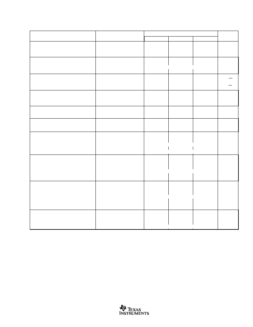
ELECTRICAL CHARACTERISTICS: V
S
= +2.7V to +5.5V
Boldface
limits apply over the specified temperature range,
T
A
=
–
40
°
C to +85
°
C.
At T
CASE
= +25
°
C, R
L
= 1k
, and connected to V
S
/2, unless otherwise noted.
NOTES: (1) See typical characteristic
“
Maximum Output Voltage vs Frequency
”
. (2) See the typical characteristic
“
Total Harmonic Distortion + Noise vs Frequency
”
.
(3) Swing to the rail is measured in final test. Under those conditions, the A
is derived from characterization. (4) See Safe Operating Area (SOA) plot. (5) See typical
characteristic
“
Overshoot vs Load Capacitance
”
. (6) External current limit setting resistor is required. See Figure 1. (7) I
is the value of the desired current limit
and is equal to 9800 (I
SET
), where I
is the current through the Current Limit Set pin (pin 3). Errors from this parameter can be calibrated out
—
see Applications
Information section. (8) V
is a voltage reference that equals the difference between the voltage of the Current Limit Set pin and V
–
, and is referenced to the negative
rail. Errors from this parameter can be calibrated out
—
see Applications Information section. (9) % Tolerance = [(I
OUT
/475)
–
I
MONITOR
]
100/I
MONITOR
.
OPA569AI
PARAMETER
CONDITION
MIN
TYP
MAX
UNITS
OFFSET VOLTAGE
Input Offset Voltage
vs Temperature
vs Power Supply
V
OS
I
O
= 0V, V
= +5V
T
=
–
40
°
C to +85
°
C
V
S
= +2.7V to +5.5V, V
CM
= (V
–
) +0.55V
±
0.5
±
1.3
12
±
2
mV
μ
V/
°
C
μ
V/V
dV
OS
/dT
PSRR
60
INPUT BIAS CURRENT
Input Bias Current
vs Temperature
Input Offset Current
I
B
±
1
±
10
pA
(doubles every 10
°
C)
±
2
I
OS
±
10
pA
NOISE
Input Voltage Noise Density, f = 1kHz
e
n
12
8
0.6
nV/
√
Hz
μ
Vp-p
fA/
√
Hz
f = 0.1Hz to 10Hz
Current Noise Density, f = 1kHz
i
n
INPUT VOLTAGE RANGE
Common-Mode Voltage Range
Common-Mode Rejection Ratio
V
Linear Operation
V
S
= +5V,
–
0.1V < V
CM
< 3.2V
V
S
= +5V,
–
0.1V < V
CM
< 5.1V
(V
–
)
–
0.1
80
60
(V+) + 0.1
V
dB
dB
CMRR
100
80
INPUT IMPEDANCE
Differential
Common-Mode
10
13
|| 4.5
10
13
|| 9
|| pF
|| pF
OPEN-LOOP GAIN
Open-Loop Voltage Gain
A
OL
0.2V
< V
O
< 4.8V, R
L
= 1k
, V
S
= +5V
0.3V
< V
O
< 4.7V, R
L
= 1.15
, V
S
= +5V
100
126
90
dB
dB
FREQUENCY RESPONSE
Gain Bandwidth Product
Slew Rate
Full-Power Bandwidth
(1)
Settling Time:
±
0.1%
Total Harmonic Distortion + Noise
(2)
GBW
SR
1.2
1.2
MHz
V/
μ
s
G = +1, V
O
= 4.0V Step
See Typical Characteristics
5
See Typical Characteristics
G =
–
1, V
O
= 4.0V Step
μ
s
THD+N
OUTPUT
Voltage Output Swing from Rail
V
O
R
= 1k
, A
> 100dB
I
O
=
±
2A, V
S
= +5V, A
OL
> 80dB
(3)
(V
–
) + 0.2
(V
–
) + 0.3
(V
S
)
±
0.02
(V
S
)
±
0.15
(V+)
–
0.2
(V+)
–
0.3
2.4
V
V
A
Maximum Continuous Current Output: dc
(4)
Capacitive Load Drive
(5)
Output Disabled
Output Impedance
C
LOAD
See Typical Characteristics
12M || 570
|| pF
CURRENT LIMIT
Output Current Limit
(6)
Current Limit Equation
R
Equation
Current Limit Tolerance
(7)
, Positive
Externally Adjustable
±
0.2 to
±
2.2
I
= I
9800
R
SET
= 9800 (1.18V/I
LIMIT
)
±
3
±
3
(V
–
) + 1.18
A
A
%
%
V
I
LIMIT
= 1A
I
LIMIT
= 1A
±
10
±
15
Negative
Voltage on Current Limit Set Pin Tolerance
(8)
(V
–
) + 1.05
(V
–
) + 1.3
OUTPUT CURRENT MONITOR (Pin 19)
Output Current Monitor
Output Current Monitor Tolerance
(9)
, Positive
I
M
I
M
=
I
O
/475
±
3
±
3
A
%
%
I
O
= +1A, R
MONITOR
= 400
I
O
=
–
1A, R
= 400
Linear Operation
±
10
±
15
Negative
Compliance Voltage Range
See Discussion on Current Monitor Section
相關(guān)PDF資料 |
PDF描述 |
|---|---|
| OPA602 | High-Speed Precision Difet OPERATIONAL AMPLIFIER |
| OPA602AM | High-Speed Precision Difet OPERATIONAL AMPLIFIER |
| OPA602AP | High-Speed Precision Difet OPERATIONAL AMPLIFIER |
| OPA602AU | High-Speed Precision Difet OPERATIONAL AMPLIFIER |
| OPA602BM | High-Speed Precision Difet OPERATIONAL AMPLIFIER |
相關(guān)代理商/技術(shù)參數(shù) |
參數(shù)描述 |
|---|---|
| OPA569AIDWP | 功能描述:運(yùn)算放大器 - 運(yùn)放 2A Pwr Op Amp Rail-To-Rail I/O RoHS:否 制造商:STMicroelectronics 通道數(shù)量:4 共模抑制比(最小值):63 dB 輸入補(bǔ)償電壓:1 mV 輸入偏流(最大值):10 pA 工作電源電壓:2.7 V to 5.5 V 安裝風(fēng)格:SMD/SMT 封裝 / 箱體:QFN-16 轉(zhuǎn)換速度:0.89 V/us 關(guān)閉:No 輸出電流:55 mA 最大工作溫度:+ 125 C 封裝:Reel |
| OPA569AIDWPG4 | 功能描述:運(yùn)算放大器 - 運(yùn)放 2A Pwr Op Amp Rail-To-Rail I/O RoHS:否 制造商:STMicroelectronics 通道數(shù)量:4 共模抑制比(最小值):63 dB 輸入補(bǔ)償電壓:1 mV 輸入偏流(最大值):10 pA 工作電源電壓:2.7 V to 5.5 V 安裝風(fēng)格:SMD/SMT 封裝 / 箱體:QFN-16 轉(zhuǎn)換速度:0.89 V/us 關(guān)閉:No 輸出電流:55 mA 最大工作溫度:+ 125 C 封裝:Reel |
| OPA569AIDWPR | 功能描述:運(yùn)算放大器 - 運(yùn)放 2A Pwr Op Amp Rail-To-Rail I/O RoHS:否 制造商:STMicroelectronics 通道數(shù)量:4 共模抑制比(最小值):63 dB 輸入補(bǔ)償電壓:1 mV 輸入偏流(最大值):10 pA 工作電源電壓:2.7 V to 5.5 V 安裝風(fēng)格:SMD/SMT 封裝 / 箱體:QFN-16 轉(zhuǎn)換速度:0.89 V/us 關(guān)閉:No 輸出電流:55 mA 最大工作溫度:+ 125 C 封裝:Reel |
| OPA569AIDWPRG4 | 功能描述:運(yùn)算放大器 - 運(yùn)放 2A Pwr Op Amp Rail-To-Rail I/O RoHS:否 制造商:STMicroelectronics 通道數(shù)量:4 共模抑制比(最小值):63 dB 輸入補(bǔ)償電壓:1 mV 輸入偏流(最大值):10 pA 工作電源電壓:2.7 V to 5.5 V 安裝風(fēng)格:SMD/SMT 封裝 / 箱體:QFN-16 轉(zhuǎn)換速度:0.89 V/us 關(guān)閉:No 輸出電流:55 mA 最大工作溫度:+ 125 C 封裝:Reel |
| OPA5723YGO | 制造商:KODENSHI 制造商全稱:KODENSHI KOREA CORP. 功能描述:Yellow Green LED Chip |
發(fā)布緊急采購(gòu),3分鐘左右您將得到回復(fù)。