- 您現(xiàn)在的位置:買賣IC網(wǎng) > PDF目錄383692 > OPA569 Power Op Amp. Output Signal Swings Within 200mV of Rails at 2A Output Current PDF資料下載
參數(shù)資料
| 型號: | OPA569 |
| 英文描述: | Power Op Amp. Output Signal Swings Within 200mV of Rails at 2A Output Current |
| 中文描述: | 功率運算放大器。輸出信號擺幅在200mV的Rails的輸出電流為2A |
| 文件頁數(shù): | 13/23頁 |
| 文件大?。?/td> | 411K |
| 代理商: | OPA569 |
OPA569
SBOS264
13
www.ti.com
Current Limit Accuracy
Internally separate circuits monitor the positive and negative
current limits. Each circuit output is compared to a single
internal reference that is set by the user with an external
resistor or a resistor/voltage source combination. The OPA569
employs a patented circuit technique to achieve an accurate
and stable current limit throughout the full output range. The
initial accuracy of the current limit is typically within 3%;
however, due to internal matching limitations, the error can
be as much as 15%. The variation of the current limit with
factors such as output current level, output voltage and
temperature is shown in the Typical Characteristics section.
When the accuracy of one current limit (sourcing or sinking)
is more important than the other, it is possible to set its
accuracy to better than 1% by adjusting the external resistor
or the applied voltage. The accuracy of the other current limit
will still be affected by internal matching.
Current Limit Flag Pin
The OPA569 features a Current Limit Flag pin (pin 4) that
can be monitored to determine when the part is in current
limit. The output signal of the current limit flag pin is compat-
ible to standard logic in single supply applications. The
output signal is a CMOS logic gate that switches from V+ to
V
–
to indicate that the amplifier is in current limit. This flag
output pin can source and sink up to 25
μ
A. Additional
parasitic capacitance between pins 3 and 4 can cause
instability at the edge of the current limit. Avoid routing these
traces in parallel close to each other.
Quiescent Current Dependence on the
Current Limit Setting
The OPA569 is a low power amplifier, with a typical 3.4mA
quiescent current (with the current limit configured for 200mA).
The quiescent current varies with on the current limit set-
ting
—
it increases 0.5mA for each additional 200mA in-
crease in the current limit, as shown in Figure 3.
FIGURE 3. Quiescent Current vs Current Limit Setting.
10
8
6
4
2
0
QUIESCENT CURRENT vs CURRENT LIMIT SETTING
Current Limit Setting (A)
Q
0
0.5
1
1.5
2
2.5
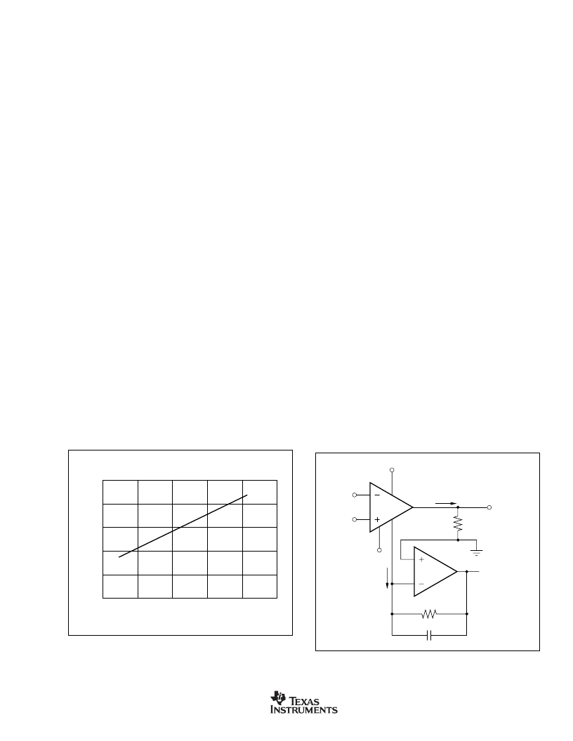
FIGURE 4. Transimpedance Amplifier to Monitor Load
Current.
OPA569
R
L
I
O
I
O
/475
I
MONITOR
V
O
V
O
=
–
1V
at I
O
= 1A
–
2.5V
5
6
19
14,
15
12,
13
R = 475
C
–
In
+In
+2.5V
OPA348
17,
18
CURRENT MONITOR
The OPA569 features an accurate output current monitor
(I
MONITOR
) without requiring the use of series resistance with
the load. This increases efficiency significantly and provides
better overall swing-to-supply performance.
An internal circuit creates a 1:475 copy of the output current.
This copy of the output current can be monitored indepen-
dently or it can be used in applications such as current
control drive, setting non-symmetric positive and negative
current limits or paralleling two or more devices for increased
output current drive. When not being used, the Current
Monitor pin may be left floating.
Some restrictions apply when using the current monitor
function. When the main amplifier is sourcing current, the
current monitor circuit must be sourcing current. Likewise,
when the main amplifier is sinking current, the current moni-
tor circuit must also be sinking current. Additionally, the
swing on the I
MONITOR
pin is smaller than the output swing.
When the amplifier is sourcing current, the voltage of the
Current Monitor pin must be at least two hundred millivolts
less than the output voltage of the amplifier. Conversely,
when the amplifier is sinking current, the voltage of the
Current Monitor pin must be at least two hundred millivolts
greater than the output voltage of the amplifier. Resistive
loads are able to meet these restrictions. Other types of
loads may cause invalid current monitor values.
A simple way to monitor the load current and meet these
requirements is to connect a resistor (with resistance less
than 400
R
L
) from the I
MONITOR
pin to the same potential to
which the other side of the load is connected. Another
method is to use a transimpedance amplifier, as shown in
Figure 4. This circuit must assure that the potential of the
I
MONITOR
pin remains in the valid voltage range by connecting
it to the same potential to which the load is connected
—
most
likely ground for dual supply or mid-supply for single-supply
applications.
相關PDF資料 |
PDF描述 |
|---|---|
| OPA602 | High-Speed Precision Difet OPERATIONAL AMPLIFIER |
| OPA602AM | High-Speed Precision Difet OPERATIONAL AMPLIFIER |
| OPA602AP | High-Speed Precision Difet OPERATIONAL AMPLIFIER |
| OPA602AU | High-Speed Precision Difet OPERATIONAL AMPLIFIER |
| OPA602BM | High-Speed Precision Difet OPERATIONAL AMPLIFIER |
相關代理商/技術參數(shù) |
參數(shù)描述 |
|---|---|
| OPA569AIDWP | 功能描述:運算放大器 - 運放 2A Pwr Op Amp Rail-To-Rail I/O RoHS:否 制造商:STMicroelectronics 通道數(shù)量:4 共模抑制比(最小值):63 dB 輸入補償電壓:1 mV 輸入偏流(最大值):10 pA 工作電源電壓:2.7 V to 5.5 V 安裝風格:SMD/SMT 封裝 / 箱體:QFN-16 轉換速度:0.89 V/us 關閉:No 輸出電流:55 mA 最大工作溫度:+ 125 C 封裝:Reel |
| OPA569AIDWPG4 | 功能描述:運算放大器 - 運放 2A Pwr Op Amp Rail-To-Rail I/O RoHS:否 制造商:STMicroelectronics 通道數(shù)量:4 共模抑制比(最小值):63 dB 輸入補償電壓:1 mV 輸入偏流(最大值):10 pA 工作電源電壓:2.7 V to 5.5 V 安裝風格:SMD/SMT 封裝 / 箱體:QFN-16 轉換速度:0.89 V/us 關閉:No 輸出電流:55 mA 最大工作溫度:+ 125 C 封裝:Reel |
| OPA569AIDWPR | 功能描述:運算放大器 - 運放 2A Pwr Op Amp Rail-To-Rail I/O RoHS:否 制造商:STMicroelectronics 通道數(shù)量:4 共模抑制比(最小值):63 dB 輸入補償電壓:1 mV 輸入偏流(最大值):10 pA 工作電源電壓:2.7 V to 5.5 V 安裝風格:SMD/SMT 封裝 / 箱體:QFN-16 轉換速度:0.89 V/us 關閉:No 輸出電流:55 mA 最大工作溫度:+ 125 C 封裝:Reel |
| OPA569AIDWPRG4 | 功能描述:運算放大器 - 運放 2A Pwr Op Amp Rail-To-Rail I/O RoHS:否 制造商:STMicroelectronics 通道數(shù)量:4 共模抑制比(最小值):63 dB 輸入補償電壓:1 mV 輸入偏流(最大值):10 pA 工作電源電壓:2.7 V to 5.5 V 安裝風格:SMD/SMT 封裝 / 箱體:QFN-16 轉換速度:0.89 V/us 關閉:No 輸出電流:55 mA 最大工作溫度:+ 125 C 封裝:Reel |
| OPA5723YGO | 制造商:KODENSHI 制造商全稱:KODENSHI KOREA CORP. 功能描述:Yellow Green LED Chip |
發(fā)布緊急采購,3分鐘左右您將得到回復。