- 您現(xiàn)在的位置:買賣IC網(wǎng) > PDF目錄359243 > MVTX2803 (Zarlink Semiconductor Inc.) Unmanaged 8-Port 1000 Mbps Ethernet Switch PDF資料下載
參數(shù)資料
| 型號: | MVTX2803 |
| 廠商: | Zarlink Semiconductor Inc. |
| 英文描述: | Unmanaged 8-Port 1000 Mbps Ethernet Switch |
| 中文描述: | 非托管8端口1000 Mbps以太網(wǎng)交換機(jī) |
| 文件頁數(shù): | 29/127頁 |
| 文件大小: | 1706K |
| 代理商: | MVTX2803 |
第1頁第2頁第3頁第4頁第5頁第6頁第7頁第8頁第9頁第10頁第11頁第12頁第13頁第14頁第15頁第16頁第17頁第18頁第19頁第20頁第21頁第22頁第23頁第24頁第25頁第26頁第27頁第28頁當(dāng)前第29頁第30頁第31頁第32頁第33頁第34頁第35頁第36頁第37頁第38頁第39頁第40頁第41頁第42頁第43頁第44頁第45頁第46頁第47頁第48頁第49頁第50頁第51頁第52頁第53頁第54頁第55頁第56頁第57頁第58頁第59頁第60頁第61頁第62頁第63頁第64頁第65頁第66頁第67頁第68頁第69頁第70頁第71頁第72頁第73頁第74頁第75頁第76頁第77頁第78頁第79頁第80頁第81頁第82頁第83頁第84頁第85頁第86頁第87頁第88頁第89頁第90頁第91頁第92頁第93頁第94頁第95頁第96頁第97頁第98頁第99頁第100頁第101頁第102頁第103頁第104頁第105頁第106頁第107頁第108頁第109頁第110頁第111頁第112頁第113頁第114頁第115頁第116頁第117頁第118頁第119頁第120頁第121頁第122頁第123頁第124頁第125頁第126頁第127頁
MVTX2803
Data Sheet
29
Zarlink Semiconductor Inc.
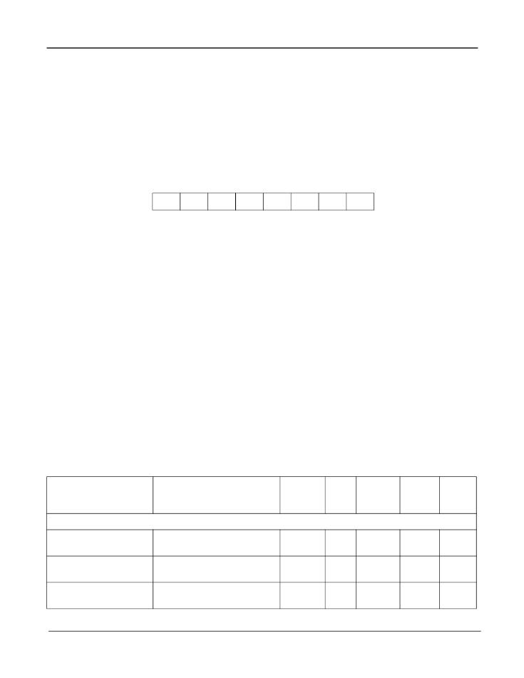
Bits [7:4]
Signal select: 0: do not select
1: select the corresponding bit
For j = 2, 3, 4, 5, the value of LED_BYTEOUT_[j] equals the logical AND of all selected bits. For j = 6, the value
is equal to the logical OR. Therefore, the programmable LEDSIG[5:2] registers allow any conjunctive formula
including any of the 4 status bits (COL, FDX, SP1, SP0) or their negations to be sent to the
LED_BYTEOUT_[5:2] pins. Similarly, the programmable LEDSIG[6] register allows any disjunctive formula
including any of the 4 status bits or their negations to be sent to pin LED_BYTEOUT_[6].
LEDSIG[7] is used for programming both LED_BYTEOUT_[1] and LED_BYTEOUT_[0]. As we will see, it has
other functions as well. The format is as follows:
10.0 Register Definition
10.1 MVTX2803AG Register Description
7
4
3
0
GP
RxD
TxD
FC
P6
RxD
TxD
FC
Bits [7]
Global output polarity: this bit controls the output polarity of all LED_BYTEOUT_ and
LED_PORT_SEL pins.
(Default 0)
0: do not invert polarity (LED_BYTEOUT_[7:0] are high activated; LED_PORT_SEL[9:0] are low
activated)
1: invert polarity (LED_BYTEOUT_[7:0] are low activated; LED_PORT_SEL[9:0] are high activated)
Bits [6:4]
Signal select:
0: do not select
1: select the corresponding bit
The value of LED_BYTEOUT_[1] equals the logical OR of all selected bits.
(Default 110)
Bit [3]
Polarity control of LED_BYTEOUT_[6]
(Default 0)
0: do not invert
1: invert
Bits [2:0]
Signal select:
0: do not select
1: select the corresponding bit
The value of LED_BYTEOUT_[0] equals the logical OR of all selected bits. (
Default 001)
Register
Description
CPU
Addr
(Hex)
R/W
I
2
C
Addr
(Hex)
Default
Notes
ETHERNET Port Control Registers – Substitute [N] with Port number (0..7)
ECR1P”N”
Port Control Register 1 for Port
N (N=0-7)
000 + 2N
R/W
000+2N
c0
ECR2P”N”
Port Control Register 2 for Port
N (N=0-7)
001 + 2N
R/W
001+2N
00
GGCONTROL0
Extra Gigabit Port Control
–port 0,1
012
R/W
N/A
00
相關(guān)PDF資料 |
PDF描述 |
|---|---|
| MVTX2803AG | Unmanaged 8-Port 1000 Mbps Ethernet Switch |
| MVTX2804 | 8-Port 1000 Mbps Ethernet Distributed Switch |
| MVTX2804AG | 8-Port 1000 Mbps Ethernet Distributed Switch |
| MVV200 | Analog IC |
| MW005A | DC-to-DC Voltage Converter |
相關(guān)代理商/技術(shù)參數(shù) |
參數(shù)描述 |
|---|---|
| MVTX2803A | 制造商:未知廠家 制造商全稱:未知廠家 功能描述:Unmanaged 8 port Gigabit Ethernet switch |
| MVTX2803AG | 制造商:ZARLINK 制造商全稱:Zarlink Semiconductor Inc 功能描述:Unmanaged 8-Port 1000 Mbps Ethernet Switch |
| MVTX2803AG2 | 制造商:Microsemi Corporation 功能描述: |
| MVTX2804 | 制造商:ZARLINK 制造商全稱:Zarlink Semiconductor Inc 功能描述:8-Port 1000 Mbps Ethernet Distributed Switch |
| MVTX2804AG | 制造商:ZARLINK 制造商全稱:Zarlink Semiconductor Inc 功能描述:8-Port 1000 Mbps Ethernet Distributed Switch |
發(fā)布緊急采購,3分鐘左右您將得到回復(fù)。