- 您現(xiàn)在的位置:買賣IC網 > PDF目錄383646 > MT9196 (Mitel Networks Corporation) Integrated Digital Phone Circuit (IDPC)(集成數字電話電路) PDF資料下載
參數資料
| 型號: | MT9196 |
| 廠商: | Mitel Networks Corporation |
| 英文描述: | Integrated Digital Phone Circuit (IDPC)(集成數字電話電路) |
| 中文描述: | 綜合數字電話電路(前列腺偶發(fā)癌)(集成數字電話電路) |
| 文件頁數: | 2/43頁 |
| 文件大小: | 278K |
| 代理商: | MT9196 |
第1頁當前第2頁第3頁第4頁第5頁第6頁第7頁第8頁第9頁第10頁第11頁第12頁第13頁第14頁第15頁第16頁第17頁第18頁第19頁第20頁第21頁第22頁第23頁第24頁第25頁第26頁第27頁第28頁第29頁第30頁第31頁第32頁第33頁第34頁第35頁第36頁第37頁第38頁第39頁第40頁第41頁第42頁第43頁
MT9196
7-136
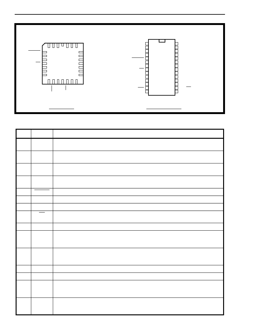
Figure 2 - Pin Connections
Pin Description
Pin #
Name
Description
1
M-
Inverting Microphone (Input).
Inverting input to microphone amplifier from the handset
microphone.
2
M+
Non-Inverting Microphone (Input).
Non-inverting input to microphone amplifier from the
handset microphone.
3
V
Bias
Bias Voltage (Output).
(V
DD
/2) volts is available at this pin for biasing external amplifiers.
Connect 0.1
μ
F capacitor to V
SSA
.
Reference voltage for codec (Output).
Nominally [(V
DD
/2)-1.5] volts. Used internally.
Connect 0.1
μ
F capacitor to V
SSA
.
Power-up Reset (Input).
CMOS compatible input with Schmitt Trigger (active low).
4
V
Ref
5
PWRST
6
IC
Internal Connection.
Tie externally to V
SS
for normal operation.
Digital Ground.
Nominally 0 volts.
7
V
SSD
CS
8
Chip Select (Input).
This input signal is used to select the device for microport data
transfers. Active low. TTL level compatible.
9
SCLK
Serial Port Synchronous Clock (Input).
Data clock for microport. TTL level compatible.
10
DATA1
Bidirectional Serial Data.
Port for microprocessor serial data transfer. In Motorola/National
mode of operation, this pin becomes the data transmit pin only and data receive is
performed on the DATA2 pin. TTL level compatible input levels.
11
DATA2
Serial Data Receive.
In Motorola/National mode of operation, this pin is used for data
receive to the IDPC. In Intel mode, serial data transmit and receive are performed on the
DATA1 pin and DATA2 is disconnected. Input level TTL compatible.
12
WD
Watchdog (Output).
Watchdog timer output. Active high.
13
IRQ
Interrupt Request (Open Drain Output).
Low true interrupt output to microcontroller.
14
D
out
Data Output.
A tri-state digital output for 8 bit wide channel data being sent to the Layer 1
device. Data is shifted out via this pin concurrent with the rising edge of BCL during the
timeslot defined by STB, or according to standard ST-BUS timing.
15
D
in
Data Input.
A digital input for 8 bit wide channel data received from the Layer 1 device.
Data is sampled on the falling edge of BCL during the timeslot defined by STB, or according
to standard ST-BUS timing. Input level is CMOS compatible.
AUXin
AUXout
MIC+
VDD
XSTAL2
HSPKR-
HSPKR+
SPKR-
SPKR+
VSS SPKR
VSSA
STB/F0i
Din
CLOCKin
M-
M+
VBias
VRef
PWRST
IC
VSSD
CS
SCLK
DATA1
DATA2
WD
IRQ
Dout
28 PIN PLCC
28 PIN SOIC/PDIP
1
6
7
8
9
10
11
12 13 14 15 16 17 18
5
4
3
2
23
22
19
20
21
24
25
26
27
28
M
M
V
V
PWRST
IC
VSSD
CS
SCLK
DATA1
DATA2
VDD
HSPKR-
HSPKR+
SPKR-
SPKR+
VSS SPKR
AUXout
A
M
V
I
D
S
C
X
D
W
17
16
15
18
19
20
28
27
26
25
24
23
22
21
1
2
3
4
5
6
7
8
9
10
11
12
13
14
相關PDF資料 |
PDF描述 |
|---|---|
| MT91L60 | 3 Volt Multi-Featured Codec (MFC)(3V 多特性編解碼器) |
| MT91L61 | 3 Volt Multi-Featured Codec (MFC)(3V 多特性編解碼器) |
| MT91L61 | ISO2-CMOS 3 Volt Multi-Featured Codec (MFC) |
| MT91L61AE | ISO2-CMOS 3 Volt Multi-Featured Codec (MFC) |
| MT91L61AN | ISO2-CMOS 3 Volt Multi-Featured Codec (MFC) |
相關代理商/技術參數 |
參數描述 |
|---|---|
| MT9196AE | 制造商:Microsemi Corporation 功能描述:INTEGRATED DGTL PHONE CIRCUIT (IDPC) 28PDIP - Rail/Tube |
| MT9196AE1 | 制造商:Microsemi Corporation 功能描述:INTEGRATED DGTL PHONE CIRCUIT (IDPC) 28PDIP - Rail/Tube 制造商:MICROSEMI CONSUMER MEDICAL PRODUCT GROUP 功能描述:IC DGTL TELEPHONE CIRCUIT 28PDIP 制造商:Microsemi Corporation 功能描述:IC DGTL TELEPHONE CIRCUIT 28PDIP |
| MT9196AP | 制造商:Microsemi Corporation 功能描述: |
| MT9196AP1 | 制造商:Microsemi Corporation 功能描述:INTEGRATED DGTL PHONE CIRCUIT (IDPC) 28PLCC - Rail/Tube 制造商:MICROSEMI CONSUMER MEDICAL PRODUCT GROUP 功能描述:IC DGTL TELEPHONE CIRCUIT 28PLCC 制造商:Microsemi Corporation 功能描述:IC DGTL TELEPHONE CIRCUIT 28PLCC |
| MT9196APR | 制造商:ZARLINK 制造商全稱:Zarlink Semiconductor Inc 功能描述:Integrated Digital Phone Circuit (IDPC) |
發(fā)布緊急采購,3分鐘左右您將得到回復。