- 您現(xiàn)在的位置:買賣IC網(wǎng) > PDF目錄359235 > MT90883 (Zarlink Semiconductor Inc.) TDM to Packet Processors PDF資料下載
參數(shù)資料
| 型號(hào): | MT90883 |
| 廠商: | Zarlink Semiconductor Inc. |
| 英文描述: | TDM to Packet Processors |
| 中文描述: | TDM到分組處理器 |
| 文件頁(yè)數(shù): | 67/97頁(yè) |
| 文件大?。?/td> | 702K |
| 代理商: | MT90883 |
第1頁(yè)第2頁(yè)第3頁(yè)第4頁(yè)第5頁(yè)第6頁(yè)第7頁(yè)第8頁(yè)第9頁(yè)第10頁(yè)第11頁(yè)第12頁(yè)第13頁(yè)第14頁(yè)第15頁(yè)第16頁(yè)第17頁(yè)第18頁(yè)第19頁(yè)第20頁(yè)第21頁(yè)第22頁(yè)第23頁(yè)第24頁(yè)第25頁(yè)第26頁(yè)第27頁(yè)第28頁(yè)第29頁(yè)第30頁(yè)第31頁(yè)第32頁(yè)第33頁(yè)第34頁(yè)第35頁(yè)第36頁(yè)第37頁(yè)第38頁(yè)第39頁(yè)第40頁(yè)第41頁(yè)第42頁(yè)第43頁(yè)第44頁(yè)第45頁(yè)第46頁(yè)第47頁(yè)第48頁(yè)第49頁(yè)第50頁(yè)第51頁(yè)第52頁(yè)第53頁(yè)第54頁(yè)第55頁(yè)第56頁(yè)第57頁(yè)第58頁(yè)第59頁(yè)第60頁(yè)第61頁(yè)第62頁(yè)第63頁(yè)第64頁(yè)第65頁(yè)第66頁(yè)當(dāng)前第67頁(yè)第68頁(yè)第69頁(yè)第70頁(yè)第71頁(yè)第72頁(yè)第73頁(yè)第74頁(yè)第75頁(yè)第76頁(yè)第77頁(yè)第78頁(yè)第79頁(yè)第80頁(yè)第81頁(yè)第82頁(yè)第83頁(yè)第84頁(yè)第85頁(yè)第86頁(yè)第87頁(yè)第88頁(yè)第89頁(yè)第90頁(yè)第91頁(yè)第92頁(yè)第93頁(yè)第94頁(yè)第95頁(yè)第96頁(yè)第97頁(yè)
MT90880/1/2/3
Data Sheet
67
Zarlink Semiconductor Inc.
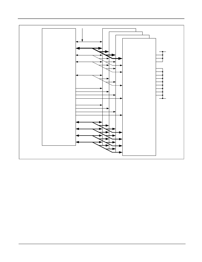
Figure 29 - Connecting the MT90880 to Multiple External Memory Devices
6.9.4 External Memory Interface Timing
The timings for the external memory interface are shown in Table 39. However, calculations to see whether the
MT90880 will be capable of operation with a particular memory device also depend on some external factors,
notably the skew on the board between the system clock S_CLK at the MT90880 and the memory device.
For example, the diagram in Figure 52 shows the memory write cycle. The MT90880 puts out the data on the
bus at time T
RDV
following the rising edge of S_CLK. This has to meet a setup time to the next rising edge of
S_CLK at the RAM (T
DS
). However, if the clock is skewed on the board such that S_CLK is slightly earlier at the
RAM than at the MT90880, the setup time is effectively increased by the amount of skew.
The maximum clock skew between devices can be determined from the following equation:
Maximum allowable clock skew
For a Micron MT58L256L32P, the minimum RAM data setup time T
DS
is 1.5 ns when using the 7.5 ns speed
grade part. T
RDV
is 10 ns (from Table 41) and with S_CLK running at 66 MHz, the clock period T
S_CLK
is 15.15
ns. Therefore,
= T
S_CLK
- T
RDV
- T
DS
Micron
TM
generic SRAM
e.g. MT58L256L32P
(256K x 3e.g. MT58L256L32P
TM
)
(256K x 3e.g. MT58L256L32P
TM
)
(256K x Ae.g. MT58L256L32P
TM
)
(25GW#
TM
)
CLK
SA0
SA1
SA
ADSC#
DQd
DQc
DQb
DQa
ADV#
MODE
ADSC#
CE2
ZZ
CE2#
BWa#
CE#
BWc#
BWd#
BWb#
OE#
GW#
TM
TM
CLK
SA0
SA1
SA
ADSC#
DQd
DQc
DQb
DQa
ADV#
MODE
CE2
GW#
ADSP#
ZZ
CE2#
BWa#
CE#
BWc#
BWd#
BWb#
OE#
GW#
CLK
SA0
SA1
SA
ADSC#
DQd
DQc
DQb
DQa
ADV#
MODE
CE2
GW#
ADSP#
ZZ
CE2#
BWa#
CE#
BWc#
BWd#
BWb#
OE#
GW#
CLK
SA0
SA1
SA
DQd
DQc
DQb
DQa
ADV#
MODE
CE2
BWE#
ADSP#
ZZ
CE2#
BWa#
CE#
BWc#
BWd#
BWb#
OE#
GW#
66 MHz
System Clock
MT9088x device
RAM_A[19:4]
RAM_D[31:24]
RAM_ADSC#
S_CLK
RAM_A[2]
RAM_A[3]
RAM_D[7:0]
RAM_D[15:8]
RAM_D[23:16]
RAM_OE[3]#
RAM_OE[0]#
RAM_OE[1]#
RAM_OE[2]#
RAM_WE[3]#
RAM_WE[0]#
RAM_WE[1]#
RAM_WE[2]#
V
DD
V
SS
相關(guān)PDF資料 |
PDF描述 |
|---|---|
| MT91600 | Programmable SLIC |
| MT91600AN | Programmable SLIC |
| MT91600AN1 | Programmable SLIC |
| MT91600ANR | Programmable SLIC |
| MT91600ANR1 | Programmable SLIC |
相關(guān)代理商/技術(shù)參數(shù) |
參數(shù)描述 |
|---|---|
| MT90883A | 制造商:ZARLINK 制造商全稱:Zarlink Semiconductor Inc 功能描述:TDM to Packet Processors |
| MT90883A/IG | 制造商:ZARLINK 制造商全稱:Zarlink Semiconductor Inc 功能描述:TDM to Packet Processors |
| MT90883BP1N | 制造商:ZARLINK 制造商全稱:Zarlink Semiconductor Inc 功能描述:TDM to Packet Processors |
| MT90883IG | 制造商:ZARLINK 制造商全稱:Zarlink Semiconductor Inc 功能描述:TDM to Packet Processors |
| MT9088IG | 制造商:ZARLINK 制造商全稱:Zarlink Semiconductor Inc 功能描述:TDM to Packet Processors |
發(fā)布緊急采購(gòu),3分鐘左右您將得到回復(fù)。