- 您現(xiàn)在的位置:買賣IC網(wǎng) > PDF目錄384756 > MT48LC8M16A2TG-7E (Micron Technology, Inc.) SYNCHRONOUS DRAM PDF資料下載
參數(shù)資料
| 型號: | MT48LC8M16A2TG-7E |
| 廠商: | Micron Technology, Inc. |
| 英文描述: | SYNCHRONOUS DRAM |
| 中文描述: | 同步DRAM |
| 文件頁數(shù): | 34/59頁 |
| 文件大?。?/td> | 1822K |
| 代理商: | MT48LC8M16A2TG-7E |
第1頁第2頁第3頁第4頁第5頁第6頁第7頁第8頁第9頁第10頁第11頁第12頁第13頁第14頁第15頁第16頁第17頁第18頁第19頁第20頁第21頁第22頁第23頁第24頁第25頁第26頁第27頁第28頁第29頁第30頁第31頁第32頁第33頁當(dāng)前第34頁第35頁第36頁第37頁第38頁第39頁第40頁第41頁第42頁第43頁第44頁第45頁第46頁第47頁第48頁第49頁第50頁第51頁第52頁第53頁第54頁第55頁第56頁第57頁第58頁第59頁
34
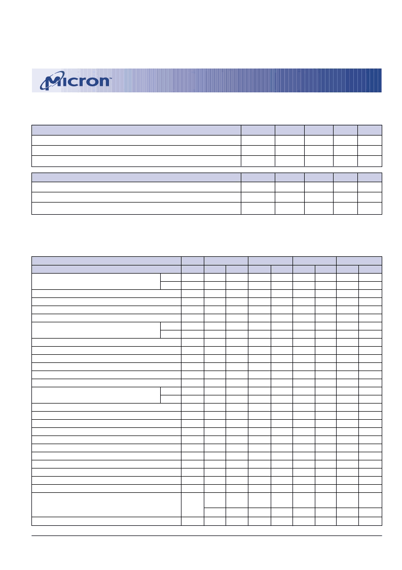
128Mb: x4, x8, x16 SDRAM
128MSDRAM_E.p65
–
Rev. E; Pub. 1/02
Micron Technology, Inc., reserves the right to change products or specifications without notice.
2001, Micron Technology, Inc.
128Mb: x4, x8, x16
SDRAM
ELECTRICAL CHARACTERISTICS AND RECOMMENDED
AC OPERATING CONDITIONS
(Notes: 5, 6, 8, 9, 11; notes appear on page 36)
AC CHARACTERISTICS
PARAMETER
Access time from CLK (pos. edge)
-7E
-75
-8E
SYMBOL
t
AC(3)
t
AC(2)
t
AH
t
AS
t
CH
t
CL
t
CK(3)
t
CK(2)
t
CKH
t
CKS
t
CMH
t
CMS
t
DH
t
DS
t
HZ(3)
t
HZ(2)
t
LZ
t
OH
t
OH
N
t
RAS
t
RC
t
RCD
t
REF
t
RFC
t
RP
t
RRD
t
T
t
WR
MIN
MAX
5.4
5.4
MIN
MAX
5.4
6
MIN
MAX
6
6
UNITS
ns
ns
ns
ns
ns
ns
ns
ns
ns
ns
ns
ns
ns
ns
ns
ns
ns
ns
ns
ns
ns
ns
ms
ns
ns
ns
ns
–
NOTES
27
CL = 3
CL = 2
Address hold time
Address setup time
CLK high-level width
CLK low-level width
Clock cycle time
0.8
1.5
2.5
2.5
7
7.5
0.8
1.5
0.8
1.5
0.8
1.5
0.8
1.5
2.5
2.5
7.5
10
0.8
1.5
0.8
1.5
0.8
1.5
1
2
3
3
8
CL = 3
CL = 2
23
23
10
1
2
1
2
1
2
CKE hold time
CKE setup time
CS#, RAS#, CAS#, WE#, DQM hold time
CS#, RAS#, CAS#, WE#, DQM setup time
Data-in hold time
Data-in setup time
Data-out high-impedance time
CL = 3
CL = 2
5.4
5.4
5.4
6
6
6
10
10
Data-out low-impedance time
Data-out hold time (load)
Data-out hold time (no load)
ACTIVE to PRECHARGE command
ACTIVE to ACTIVE command period
ACTIVE to READ or WRITE delay
Refresh period (4,096 rows)
AUTO REFRESH period
PRECHARGE command period
ACTIVE bank
a
to ACTIVE bank
b
command
Transition time
WRITE recovery time
1
3
1
3
1
3
1.8
37
60
15
1.8
44
66
20
1.8
50
70
20
28
120,000
120,000
120,000
64
64
64
66
15
14
0.3
66
20
15
0.3
70
20
20
0.3
1.2
1.2
1.2
7
1 CLK +
7ns
14
67
1 CLK +
7.5ns
15
75
1 CLK +
7ns
15
80
24
ns
ns
25
20
Exit SELF REFRESH to ACTIVE command
t
XSR
CAPACITANCE
(Note: 2; notes appear on page 36)
PARAMETER - TSOP “TG” Package
Input Capacitance: CLK
Input Capacitance: All other input-only pins
Input/Output Capacitance: DQs
SYMBOL
C
I
1
C
I
2
C
IO
MIN
2.5
2.5
4.0
MAX
3.5
3.8
6.0
UNITS NOTES
pF
pF
pF
29
30
31
PARAMETER - FBGA “FB” Package
Input Capacitance: CLK
Input Capacitance: All other input-only pins
Input/Output Capacitance: DQs
SYMBOL
C
I
1
C
I
2
C
IO
MIN
1.5
1.5
3.0
MAX
3.5
3.8
6.0
UNITS NOTES
pF
pF
pF
34
35
36
相關(guān)PDF資料 |
PDF描述 |
|---|---|
| MT48LC8M16A2TG-7EIT | SYNCHRONOUS DRAM |
| MT48LC8M16A2TG-7EL | SYNCHRONOUS DRAM |
| MT48LC8M16A2TG-7ELIT | SYNCHRONOUS DRAM |
| MT48LC8M16A2TG-8E | SYNCHRONOUS DRAM |
| MT48LC8M16A2TG-8EIT | SYNCHRONOUS DRAM |
相關(guān)代理商/技術(shù)參數(shù) |
參數(shù)描述 |
|---|
發(fā)布緊急采購,3分鐘左右您將得到回復(fù)。