- 您現(xiàn)在的位置:買賣IC網(wǎng) > PDF目錄384755 > MT48LC16M16A2 (Micron Technology, Inc.) SYNCHRONOUS DRAM PDF資料下載
參數(shù)資料
| 型號(hào): | MT48LC16M16A2 |
| 廠商: | Micron Technology, Inc. |
| 英文描述: | SYNCHRONOUS DRAM |
| 中文描述: | 同步DRAM |
| 文件頁數(shù): | 27/62頁 |
| 文件大?。?/td> | 1517K |
| 代理商: | MT48LC16M16A2 |
第1頁第2頁第3頁第4頁第5頁第6頁第7頁第8頁第9頁第10頁第11頁第12頁第13頁第14頁第15頁第16頁第17頁第18頁第19頁第20頁第21頁第22頁第23頁第24頁第25頁第26頁當(dāng)前第27頁第28頁第29頁第30頁第31頁第32頁第33頁第34頁第35頁第36頁第37頁第38頁第39頁第40頁第41頁第42頁第43頁第44頁第45頁第46頁第47頁第48頁第49頁第50頁第51頁第52頁第53頁第54頁第55頁第56頁第57頁第58頁第59頁第60頁第61頁第62頁
27
256Mb: x4, x8, x16 SDRAM
256MSDRAM_E.p65
–
Rev. E; Pub. 3/02
Micron Technology, Inc., reserves the right to change products or specifications without notice.
2002, Micron Technology, Inc.
256Mb: x4, x8, x16
SDRAM
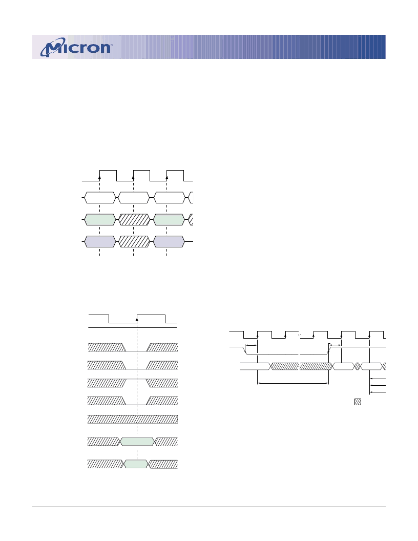
Fixed-length or full-page WRITE bursts can be trun-
cated with the BURST TERMINATE command. When
truncating a WRITE burst, the input data applied coin-
cident with the BURST TERMINATE command will be
ignored. The last data written (provided that DQM is
LOW at that time) will be the input data applied one
clock previous to the BURST TERMINATE command.
This is shown in Figure 19, where data
n
is the last
desired data element of a longer burst.
Figure 21
Power-Down
DON
’
T CARE
tRAS
tRC
tRCD
All banks idle
Input buffers gated off
Exit power-down mode.
(
)
(
)
(
)
(
)
(
)
(
)
tCKS
> tCKS
COMMAND
NOP
ACTIVE
Enter power-down mode.
NOP
CLK
CKE
(
)
(
)
(
)
(
)
Figure 20
PRECHARGE Command
Figure 19
Terminating a WRITE Burst
CLK
DQ
T2
T1
T0
COMMAND
ADDRESS
BANK,
COL
n
WRITE
BURST
TERMINATE
NEXT
COMMAND
D
IN
n
(ADDRESS)
(DATA)
NOTE:
DQMs are LOW.
PRECHARGE
The PRECHARGE command (see Figure 20) is used
to deactivate the open row in a particular bank or the
open row in all banks. The bank(s) will be available for
a subsequent row access some specified time (
t
RP) af-
ter the PRECHARGE command is issued. Input A10
determines whether one or all banks are to be
precharged, and in the case where only one bank is to
be precharged, inputs BA0, BA1 select the bank. When
all banks are to be precharged, inputs BA0, BA1 are
treated as “Don’t Care.” Once a bank has been
precharged, it is in the idle state and must be activated
prior to any READ or WRITE commands being issued to
that bank.
POWER-DOWN
Power-down occurs if CKE is registered LOW coinci-
dent with a NOP or COMMAND INHIBIT when no ac-
cesses are in progress. If power-down occurs when all
banks are idle, this mode is referred to as precharge
power-down; if power-down occurs when there is a row
active in any bank, this mode is referred to as active
power-down. Entering power-down deactivates the in-
put and output buffers, excluding CKE, for maximum
power savings while in standby. The device may not
remain in the power-down state longer than the re-
fresh period (64ms) since no refresh operations are
performed in this mode.
The power-down state is exited by registering a NOP
or COMMAND INHIBIT and CKE HIGH at the desired
clock edge (meeting
t
CKS). See Figure 21.
CS#
WE#
CAS#
RAS#
CKE
CLK
A10
HIGH
All Banks
Bank Selected
A0-A9, A11, A12
BA0, BA1
ABANK
相關(guān)PDF資料 |
PDF描述 |
|---|---|
| MT48LC64M4A2 | SYNCHRONOUS DRAM |
| MT48LC4M32B2 | SYNCHRONOUS DRAM |
| MT48LC4M32LFFC | SYNCHRONOUS DRAM |
| MT48LC64M8A2 | SYNCHRONOUS DRAM |
| MT48LC32M16A2 | SYNCHRONOUS DRAM |
相關(guān)代理商/技術(shù)參數(shù) |
參數(shù)描述 |
|---|
發(fā)布緊急采購(gòu),3分鐘左右您將得到回復(fù)。