- 您現(xiàn)在的位置:買賣IC網(wǎng) > PDF目錄384742 > MMDF1N05ER2G (ON SEMICONDUCTOR) Power MOSFET 1 Amp, 50 Volts N-Channel SO-8, Dual PDF資料下載
參數(shù)資料
| 型號: | MMDF1N05ER2G |
| 廠商: | ON SEMICONDUCTOR |
| 元件分類: | 功率晶體管 |
| 英文描述: | Power MOSFET 1 Amp, 50 Volts N-Channel SO-8, Dual |
| 中文描述: | 2 A, 50 V, 0.3 ohm, 2 CHANNEL, N-CHANNEL, Si, POWER, MOSFET |
| 封裝: | SO-8 |
| 文件頁數(shù): | 1/5頁 |
| 文件大小: | 83K |
| 代理商: | MMDF1N05ER2G |
Semiconductor Components Industries, LLC, 2006
February, 2006 Rev. 8
1
Publication Order Number:
MMDF1N05E/D
MMDF1N05E
Power MOSFET
1 Amp, 50 Volts
NChannel SO8, Dual
These miniature surface mount MOSFETs feature ultra low R
DS(on)
and true logic level performance. They are capable of withstanding
high energy in the avalanche and commutation modes and the
draintosource diode has a low reverse recovery time. MiniMOS
devices are designed for use in low voltage, high speed switching
applications where power efficiency is important. Typical applications
are dcdc converters, and power management in portable and battery
powered products such as computers, printers, cellular and cordless
phones. They can also be used for low voltage motor controls in mass
storage products such as disk drives and tape drives. The avalanche
energy is specified to eliminate the guesswork in designs where
inductive loads are switched and offer additional safety margin against
unexpected voltage transients.
Features
Ultra Low R
DS(on)
Provides Higher Efficiency and Extends Battery Life
Logic Level Gate Drive Can Be Driven by Logic ICs
Miniature SO8 Surface Mount Package Saves Board Space
Diode Is Characterized for Use In Bridge Circuits
Diode Exhibits High Speed
Avalanche Energy Specified
Mounting Information for SO8 Package Provided
I
DSS
Specified at Elevated Temperature
PbFree Package is Available
MAXIMUM RATINGS
(T
J
= 25
°
C unless otherwise noted)
Rating
Symbol
Value
Unit
DraintoSource Voltage
V
DS
V
GS
I
D
I
DM
E
AS
50
V
GatetoSource Voltage Continuous
±
20
V
Drain Current Continuous
Drain Current
Pulsed
2.0
10
A
Single Pulse DraintoSource Avalanche
Energy Starting T
= 25
°
C
(V
DD
= 25 V, V
GS
= 10 V, I
L
= 2 Apk)
Operating and Storage Temperature Range
300
mJ
T
J
, T
stg
P
D
R
JA
55 to 150
°
C
Total Power Dissipation @ T
A
= 25
°
C
Thermal Resistance, JunctiontoAmbient
(Note 1)
2.0
W
62.5
°
C/W
Maximum Temperature for Soldering,
Time in Solder Bath
T
L
260
10
°
C
Sec
Maximum ratings are those values beyond which device damage can occur.
Maximum ratings applied to the device are individual stress limit values (not
normal operating conditions) and are not valid simultaneously. If these limits are
exceeded, device functional operation is not implied, damage may occur and
reliability may be affected.
1. Mounted on 2
″
square FR4 board (1
″
sq. 2 oz. Cu 0.06
″
thick single sided) with
one die operating, 10 sec. max.
Source1
1
2
3
4
8
7
6
5
Top View
Gate1
Source2
Gate2
Drain1
Drain1
Drain2
Drain2
1 AMPERE, 50 VOLTS
R
DS(on)
= 300 m
Device
Package
Shipping
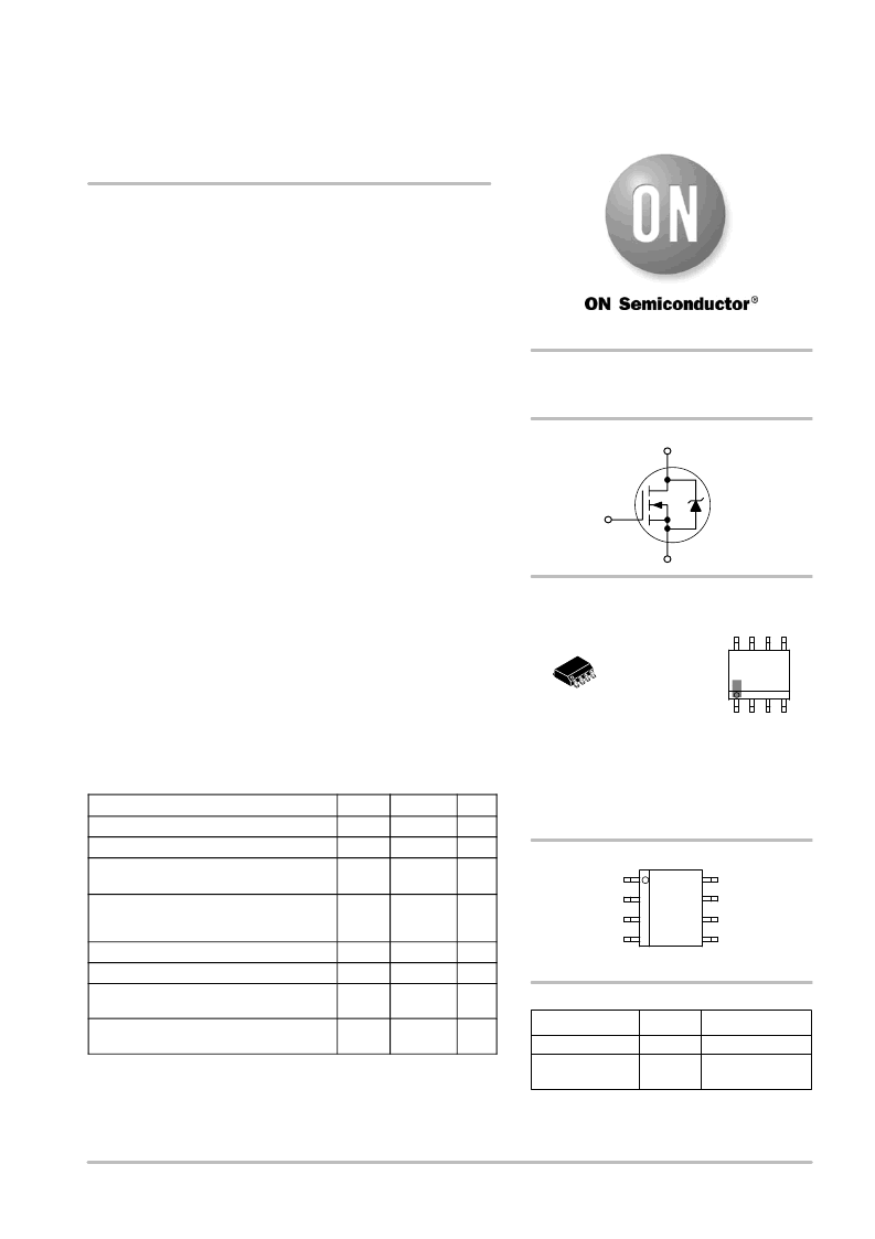
ORDERING INFORMATION
MMDF1N05ER2
SO8
2,500/Tape & Reel
NChannel
D
S
G
PIN ASSIGNMENT
http://onsemi.com
MMDF1N05ER2G
SO8
(PbFree)
2,500/Tape & Reel
For information on tape and reel specifications,
including part orientation and tape sizes, please
refer to our Tape and Reel Packaging Specifications
Brochure, BRD8011/D.
SO8
CASE 751
STYLE 11
MARKING
DIAGRAM
F1N05
A
Y
WW
= Device Code
= Assembly Location
= Year
= Work Week
= PbFree Package
(Note: Microdot may be in either location)
F1N05
AYWW
1
8
1
8
相關(guān)PDF資料 |
PDF描述 |
|---|---|
| MMDF2C03HDR2 | Power MOSFET 2 Amps, 30 Volts Complementary SO-8, Dual |
| MMDF2C03HDR2G | Power MOSFET 2 Amps, 30 Volts Complementary SO-8, Dual |
| MMDF3N02HDR2 | Power MOSFET 3 Amps, 20 Volts N-Channel SO-, DuaL |
| MMDL301T1 | cable |
| MMDL301 | Silicon Hot-Carrier Diodes |
相關(guān)代理商/技術(shù)參數(shù) |
參數(shù)描述 |
|---|---|
| MMDF1N05ER2G | 制造商:ON Semiconductor 功能描述:MOSFET |
| MMDF2C01HD | 制造商:MOTOROLA 制造商全稱:Motorola, Inc 功能描述:COMPLEMENTARY DUAL TMOS POWER FET 2.0 AMPERES 12 VOLTS |
| MMDF2C02E | 制造商:MOTOROLA 制造商全稱:Motorola, Inc 功能描述:COMPLEMENTARY DUAL TMOS POWER FET 2.5 AMPERES 25 VOLTS |
| MMDF2C02HD | 制造商:MOTOROLA 制造商全稱:Motorola, Inc 功能描述:COMPLEMENTARY DUAL TMOS POWER FET 2.0 AMPERES 20 VOLTS |
| MMDF2C02HDR2 | 制造商:ON Semiconductor 功能描述: 制造商:Motorola Inc 功能描述: |
發(fā)布緊急采購,3分鐘左右您將得到回復(fù)。