- 您現(xiàn)在的位置:買賣IC網(wǎng) > PDF目錄98023 > MM908E625ACDWB (FREESCALE SEMICONDUCTOR INC) 8-BIT, FLASH, 8 MHz, MICROCONTROLLER, PDSO54 PDF資料下載
參數(shù)資料
| 型號(hào): | MM908E625ACDWB |
| 廠商: | FREESCALE SEMICONDUCTOR INC |
| 元件分類: | 微控制器/微處理器 |
| 英文描述: | 8-BIT, FLASH, 8 MHz, MICROCONTROLLER, PDSO54 |
| 封裝: | 17.90 X 7.50 MM, 0.65 MM PITCH, PLASTIC, SOIC-54 |
| 文件頁數(shù): | 32/49頁 |
| 文件大小: | 907K |
| 代理商: | MM908E625ACDWB |
第1頁第2頁第3頁第4頁第5頁第6頁第7頁第8頁第9頁第10頁第11頁第12頁第13頁第14頁第15頁第16頁第17頁第18頁第19頁第20頁第21頁第22頁第23頁第24頁第25頁第26頁第27頁第28頁第29頁第30頁第31頁當(dāng)前第32頁第33頁第34頁第35頁第36頁第37頁第38頁第39頁第40頁第41頁第42頁第43頁第44頁第45頁第46頁第47頁第48頁第49頁
Analog Integrated Circuit Device Data
38
Freescale Semiconductor
908E625
FUNCTIONAL DEVICE OPERATION
LOGIC COMMANDS AND REGISTERS
SYSTEM CONTROL REGISTER (SYSCTL)
Power Stages On Bit (PSON)
This read/write bit enables the power stages (half-bridges,
high side, LIN transmitter, Analog Input PA1 current sources,
and HVDD output). Reset clears the PSON bit.
1 = Power stages enabled.
0 = Power stages disabled.
LIN Slew Rate Selection Bits (SRS0:SRS1)
These read/write bits enable the user to select the
appropriate LIN slew rate for different baud rate
configurations as shown in Table 11.
The high speed slew rates are used, for example, for
programming via the LIN and are not intended for use in the
application.
Go to STOP Mode Bit (GS)
This write-only bit instructs the 908E625 to power down
and go into STOP mode. Reset or CPU interrupt requests
clear the GS bit.
1 = Power down and go into STOP mode
0 = Not in STOP mode
SYSTEM STATUS REGISTER (SYSSTAT)
Hall-Effect Sensor Input Pin Overcurrent Flag Bit
(HP_OCF)
This read/write flag is set on an overcurrent condition at
one of the Hall-effect sensor input pins. Clear HP_OCF and
enable the output by writing a Logic [1] to the HP_OCF flag.
Reset clears the HP_OCF bit. Writing a Logic [0] to HP_OCF
has no effect.
1 = Overcurrent condition on Hall-effect sensor input pin
has occurred
0 = No overcurrent condition on Hall-effect sensor input
pin has occurred
LIN Current Limitation Bit (LINCL)
This read-only bit is set if the LIN transmitter operates in
current limitation region. Due to excessive power dissipation
in the transmitter, software is advised to turn the transmitter
off immediately.
1 = Transmitter operating in current limitation region
0 = Transmitter not operating in current limitation region
HVDD Output Overcurrent Flag Bit (HVDD_OCF)
This read/write flag is set on an overcurrent condition at
the HVDD pin. Clear HVDD_OCF and enable the output by
writing a Logic [1] to the HVDD_OCF Flag. Reset clears the
HVDD_OCF bit. Writing a Logic [0] to HVDD_OCF has no
effect.
1 = Overcurrent condition on HVDD has occurred
0 = No overcurrent condition on HVDD has occurred
High-Side Overcurrent Flag Bit (HS_OCF)
This read/write flag is set on an overcurrent condition at
the high-side driver. Clear HS_OCF and enable the high-side
driver by writing a Logic [1] to HS_OCF. Reset clears the
HS_OCF bit. Writing a Logic [0] to HS_OCF has no effect.
1 = Overcurrent condition on high-side drivers has
occurred
0 = No overcurrent condition on high-side drivers has
occurred
Low-Voltage Bit (LVF)
This read only bit is a copy of the LVF bit in the Interrupt
Flag Register.
1 = Low-voltage condition has occurred
0 = No low-voltage condition has occurred
High-Voltage Sensor Bit (HVF)
This read-only bit is a copy of the HVF bit in the Interrupt
Flag Register.
1 = High-voltage condition has occurred
0 = No high-voltage condition has occurred
H-Bridge Overcurrent Flag Bit (HB_OCF)
This read / write flag is set on an overcurrent condition at
the H-Bridges. Clear HB_OCF and enable the H-Bridge
driver by writing a Logic [1] to HB_OCF. Reset clears the
HB_OCF bit. Writing a Logic [0] to HB_OCF has no effect.
1 = Overcurrent condition on H-Bridges has occurred
0 = No overcurrent condition on H-Bridges has occurred
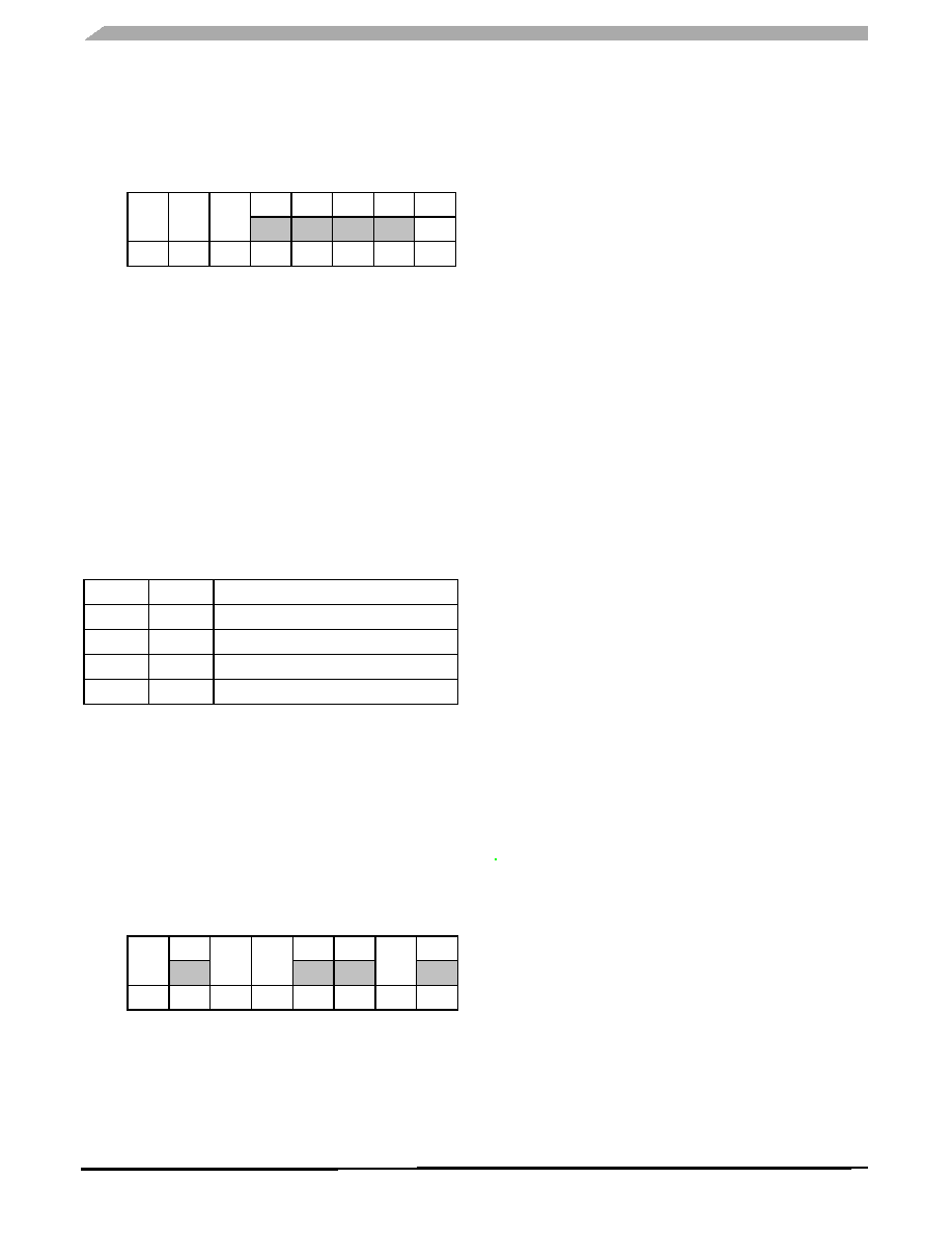
Register Name and Address: SYSCTL - $03
Bits
7
6
5
4
3
2
1
0
Read
PSON SRS1
SRS0
0
Write
GS
Reset
00
Table 11. LIN Slew Rate Selection Bits
SRS1
SRS0
LIN Slew Rate
0
Initial Slew Rate (20 kBaud)
0
1
Slow Slew Rate (10 kBaud)
1
0
High Speed II (8x)
1
High Speed I (4x)
Register Name and Address: SYSSTAT - $0c
Bits
7
6
5
4
3
2
1
0
Read
HP_
OCF
LINCL
HVDD
_OCF
HS_
OCF
LVF
HVF
HB_
OCF
HTF
Write
Reset
0000
相關(guān)PDF資料 |
PDF描述 |
|---|---|
| MMBD1010LT3 | 0.2 A, 2 ELEMENT, SILICON, SIGNAL DIODE, TO-236AB |
| MMBD3000T1 | 0.2 A, SILICON, SIGNAL DIODE |
| MMBD1000LT3 | 0.2 A, SILICON, SIGNAL DIODE, TO-236AB |
| MMBD3005T1 | 0.2 A, 2 ELEMENT, SILICON, SIGNAL DIODE |
| MMBD352WT3 | SILICON, UHF BAND, MIXER DIODE |
相關(guān)代理商/技術(shù)參數(shù) |
參數(shù)描述 |
|---|---|
| MM908E625ACDWB/R2 | 制造商:MOTOROLA 制造商全稱:Motorola, Inc 功能描述:Integrated Quad Half H-Bridge with Power Supply, Embedded MCU, and LIN Serial Communication |
| MM908E625ACEK | 功能描述:8位微控制器 -MCU Quad Half H-Bridge with P/S, HC08, LIN RoHS:否 制造商:Silicon Labs 核心:8051 處理器系列:C8051F39x 數(shù)據(jù)總線寬度:8 bit 最大時(shí)鐘頻率:50 MHz 程序存儲(chǔ)器大小:16 KB 數(shù)據(jù) RAM 大小:1 KB 片上 ADC:Yes 工作電源電壓:1.8 V to 3.6 V 工作溫度范圍:- 40 C to + 105 C 封裝 / 箱體:QFN-20 安裝風(fēng)格:SMD/SMT |
| MM908E625ACPEK | 功能描述:8位微控制器 -MCU R0 HI-BRDG EMBED MCU LIN RoHS:否 制造商:Silicon Labs 核心:8051 處理器系列:C8051F39x 數(shù)據(jù)總線寬度:8 bit 最大時(shí)鐘頻率:50 MHz 程序存儲(chǔ)器大小:16 KB 數(shù)據(jù) RAM 大小:1 KB 片上 ADC:Yes 工作電源電壓:1.8 V to 3.6 V 工作溫度范圍:- 40 C to + 105 C 封裝 / 箱體:QFN-20 安裝風(fēng)格:SMD/SMT |
| MM908E626 | 制造商:FREESCALE 制造商全稱:Freescale Semiconductor, Inc 功能描述:Integrated Stepper Motor Driver with Embedded MCU and LIN Serial Communication |
| MM908E626AVDWB | 功能描述:馬達(dá)/運(yùn)動(dòng)/點(diǎn)火控制器和驅(qū)動(dòng)器 QUADSTEPPER RoHS:否 制造商:STMicroelectronics 產(chǎn)品:Stepper Motor Controllers / Drivers 類型:2 Phase Stepper Motor Driver 工作電源電壓:8 V to 45 V 電源電流:0.5 mA 工作溫度:- 25 C to + 125 C 安裝風(fēng)格:SMD/SMT 封裝 / 箱體:HTSSOP-28 封裝:Tube |
發(fā)布緊急采購,3分鐘左右您將得到回復(fù)。