- 您現(xiàn)在的位置:買賣IC網(wǎng) > PDF目錄359645 > MCZ33742SEGR2 (飛思卡爾半導體(中國)有限公司) System Basis Chip (SBC) with Enhanced High-Speed CAN Transceiver PDF資料下載
參數(shù)資料
| 型號: | MCZ33742SEGR2 |
| 廠商: | 飛思卡爾半導體(中國)有限公司 |
| 元件分類: | CAN |
| 英文描述: | System Basis Chip (SBC) with Enhanced High-Speed CAN Transceiver |
| 中文描述: | 系統(tǒng)基礎(chǔ)芯片的增強型(SBC)的高速CAN收發(fā)器 |
| 文件頁數(shù): | 42/65頁 |
| 文件大?。?/td> | 1158K |
| 代理商: | MCZ33742SEGR2 |
第1頁第2頁第3頁第4頁第5頁第6頁第7頁第8頁第9頁第10頁第11頁第12頁第13頁第14頁第15頁第16頁第17頁第18頁第19頁第20頁第21頁第22頁第23頁第24頁第25頁第26頁第27頁第28頁第29頁第30頁第31頁第32頁第33頁第34頁第35頁第36頁第37頁第38頁第39頁第40頁第41頁當前第42頁第43頁第44頁第45頁第46頁第47頁第48頁第49頁第50頁第51頁第52頁第53頁第54頁第55頁第56頁第57頁第58頁第59頁第60頁第61頁第62頁第63頁第64頁第65頁
Analog Integrated Circuit Device Data
Freescale Semiconductor
42
33742
FUNCTIONAL DEVICE OPERATION
LOGIC COMMANDS AND REGISTERS
LOGIC COMMANDS AND REGISTERS
SPI INTERFACE AND REGISTER DESCRIPTION
DATA FORMAT DESCRIPTION
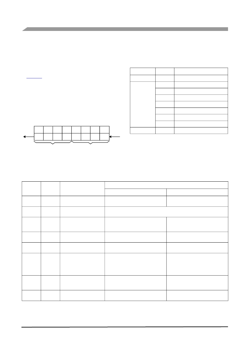
Figure 27
illustrates an 8-bit byte corresponding to the
8 bits in a SPI register. The first three bits are used to identify
the internal SBC register address. Bit 4 is a read/write bit.
The last four bits are data sent from the MCU to the SBC or
read back from the 33742 to the MCU.
The state of the MISO has no significance during the write
operation. However, during a read operation the final four bits
of MISO have meaning; namely, they contain the content of
the accessed register.
Figure 27. Data Format Description.
REGISTER DESCRIPTIONS
The following tables in this section describe the SPI
register list and register bit meaning. Register reset values
are also described, along with the reset condition. A reset
condition is the condition causing the bit to be set at the reset
value.
Bit 7
Bit 5
Bit 3
Bit 4
Bit 2
Bit 6
Bit 1
Bit 0
A2
A0
D3
R/W
D2
A1
D1
D0
MISO
MOSI
Address
Data
Note
Read operation: R/W bit = logic [0]
Write operation: R/W = logic [1]
:
Table 13. Possible Reset Conditions
Condition
Name
Definition
33742 Reset
POR
Power-ON Reset
33742 Mode
Transition
NR2R
Normal Request to Reset Mode
NR2N
Normal Request to Normal Mode
NR2STB
Normal Request to Standby Mode
N2R
Normal to Reset Mode
STB2R
Standby to Reset Mode
STO2R
Stop to Reset Mode
STO2NR
Stop to Normal Request
33742 Mode
RESET
33742S in Reset Mode
Table 14. List of Registers
Register
Address
Formal Name
and Link
Comment and Use
Write
Read
MCR
$000
Mode Control Register (MCR)
on page 43
Selection for Normal, Standby, Sleep,
Stop, and Debug modes
BATFAIL, general failure, VDD pre-
warning, and Watchdog flag
RCR
$001
Reset Control Register (RCR)
on page 44
Configuration for reset voltage level, CAN Sleep and Stop modes
CAN
$010
CAN Register (CAN) on page
44
CAN slew rate, Sleep and Wake-Up
enable/disable modes, drive enable after
failure
CAN wake-up and CAN failure status bits
IOR
$011
Input Output Register (IOR)
on page 45
HS (high-side switch) control in Normal
and Standby mode
HS overtemperature bit, VSUP, and V2
LOW status
WUR
$100
on page 46
Control of wake-up input polarity
Wake-up input and real time Lx input
state
TIM
$101
Timing Register (TIM1 2) on
page 47
TIM1: Watchdog timing control, Watch-
dog Window (WDW) or Watchdog Tim-
eout (WTO) mode
TIM2: Cyclic Sense and Forced Wake-
Up timing selection
CANL and TXD failure reporting
LPC
$110
Low Power Control Register
(LPC) on page 49
Control HS periodic activation in Sleep
and Stop modes, Forced Wake-Up mode
activation, CAN-INT mode selection
CANH and RXD failure reporting
INTR
$111
Interrupt Register (INTR) on
page 51
Enable or Disable of Interrupts
Interrupt source
相關(guān)PDF資料 |
PDF描述 |
|---|---|
| MC68HC908GR8BMFA | Microcontrollers |
| MC68HC908GR8BVFA | Microcontrollers |
| MC68HC908QT2A | Microcontrollers |
| MC68HC908QT4A | Microcontrollers |
| MC68HC908QY1A | Microcontrollers |
相關(guān)代理商/技術(shù)參數(shù) |
參數(shù)描述 |
|---|---|
| MCZ33780EG | 功能描述:多路器開關(guān) IC DBUS MASTER RoHS:否 制造商:Texas Instruments 通道數(shù)量:1 開關(guān)數(shù)量:4 開啟電阻(最大值):7 Ohms 開啟時間(最大值): 關(guān)閉時間(最大值): 傳播延遲時間:0.25 ns 工作電源電壓:2.3 V to 3.6 V 工作電源電流: 最大工作溫度:+ 85 C 安裝風格:SMD/SMT 封裝 / 箱體:UQFN-16 |
| MCZ33780EG | 制造商:Freescale Semiconductor 功能描述:DUAL DBUS MASTER INTERFACE 16SOIC |
| MCZ33780EGR2 | 功能描述:多路器開關(guān) IC DBUS MASTER RoHS:否 制造商:Texas Instruments 通道數(shù)量:1 開關(guān)數(shù)量:4 開啟電阻(最大值):7 Ohms 開啟時間(最大值): 關(guān)閉時間(最大值): 傳播延遲時間:0.25 ns 工作電源電壓:2.3 V to 3.6 V 工作電源電流: 最大工作溫度:+ 85 C 安裝風格:SMD/SMT 封裝 / 箱體:UQFN-16 |
| MCZ33781EK | 功能描述:輸入/輸出控制器接口集成電路 DBUS2 MASTER STND RoHS:否 制造商:Silicon Labs 產(chǎn)品: 輸入/輸出端數(shù)量: 工作電源電壓: 最大工作溫度:+ 85 C 最小工作溫度:- 40 C 安裝風格:SMD/SMT 封裝 / 箱體:QFN-64 封裝:Tray |
| MCZ33781EKR2 | 功能描述:輸入/輸出控制器接口集成電路 DBUS2 MASTER STND RoHS:否 制造商:Silicon Labs 產(chǎn)品: 輸入/輸出端數(shù)量: 工作電源電壓: 最大工作溫度:+ 85 C 最小工作溫度:- 40 C 安裝風格:SMD/SMT 封裝 / 箱體:QFN-64 封裝:Tray |
發(fā)布緊急采購,3分鐘左右您將得到回復。